Supermicro C7X99-OCE-F Manual
Supermicro
Bundkort
C7X99-OCE-F
Læs nedenfor 📖 manual på dansk for Supermicro C7X99-OCE-F (147 sider) i kategorien Bundkort. Denne guide var nyttig for 28 personer og blev bedømt med 4.5 stjerner i gennemsnit af 2 brugere
Side 1/147

C7X99-OCE
C7X99-OCE-F
USER’S MANUAL
Revision 1.1

The information in this User’s Manual has been carefully reviewed and is believed to be accurate. The
vendor assumes no responsibility for any inaccuracies that may be contained in this document, makes
no commitment to update or to keep current the information in this manual, or to notify any person
or organization of the updates. Please Note: For the most up-to-date version of this manual,
please see our web site at www.supermicro.com.
Super Micro Computer, Inc. ("Supermicro") reserves the right to make changes to the product de-
scribed in this manual at any time and without notice. This product, including software and documenta-
tion, is the property of Supermicro and/or its licensors, and is supplied only under a license. Any use or
reproduction of this product is not allowed, except as expressly permitted by the terms of said license.
IN NO EVENT WILL SUPERMICRO BE LIABLE FOR DIRECT, INDIRECT, SPECIAL, INCIDEN-
TAL, SPECULATIVE OR CONSEQUENTIAL DAMAGES ARISING FROM THE USE OR INABILITY
TO USE THIS PRODUCT OR DOCUMENTATION, EVEN IF ADVISED OF THE POSSIBILITY OF
SUCH DAMAGES. IN PARTICULAR, SUPERMICRO SHALL NOT HAVE LIABILITY FOR ANY
HARDWARE, SOFTWARE, OR DATA STORED OR USED WITH THE PRODUCT, INCLUDING THE
COSTS OF REPAIRING, REPLACING, INTEGRATING, INSTALLING OR RECOVERING SUCH
HARDWARE, SOFTWARE, OR DATA.
Any disputes arising between manufacturer and customer shall be governed by the laws of Santa
Clara County in the State of California, USA. The State of California, County of Santa Clara shall be
the exclusive venue for the resolution of any such disputes. Super Micro's total liability for all claims
will not exceed the price paid for the hardware product.
FCC Statement: This equipment has been tested and found to comply with the limits for a class B
digital device, pursuant to Part 15 of the FCC Rules. These limits are designed to provide reasonable
protection against harmful interference in a residential installation. This equipment generates, uses,
and can radiate radio frequency energy and, if not installed and used in accordance with the instruc-
tions, may cause harmful interference to radio communications. However, there is no guarantee that
interference will not occur in a particular installation. If this equipment does cause harmful interfer-
ence to radio or television reception, which can be determined by turning the equipment off and on,
the user is encouraged to try to correct the interference by one or more of the following measures:
• Reorient or relocate the receiving antenna.
• Increase the separation between the equipment and receiver.
• Connect the equipment to an outlet on a circuit different from that to which the
receiver is connected.
• Consult the authorized dealer or an experienced radio/TV technician for help.
California Best Management Practices Regulations for Perchlorate Materials: This Perchlorate warning
applies only to products containing CR (Manganese Dioxide) Lithium coin cells. “Perchlorate Material-
special handling may apply. See www.dtsc.ca.gov/hazardouswaste/perchlorate”
WARNING: Handling of lead solder materials used
in this product may expose you to lead, a chemi-
cal known to the State of California to cause birth
defects and other reproductive harm.
Manual Revision 1.1
Release Date: September 21, 2016
Unless you request and receive written permission from Super Micro Computer, Inc., you may not
copy any part of this document.
Information in this document is subject to change without notice. Other products and companies
referred to herein are trademarks or registered trademarks of their respective companies or mark
holders.
Copyright © 2016 by Super Micro Computer, Inc. All rights reserved.
Printed in the United States of America

iii
Preface
This manual is written for system integrators, PC technicians and
knowledgeable PC users. It provides information for the installation and
use of the C7X99-OCE/C7X99-OCE-F motherboard.
Manual Organization
Chapter 1 describes the features, specications and performance of
the motherboard, and provides detailed information on the Intel X99
Express chipset.
Chapter 2 provides hardware installation instructions. Read this chap-
ter when installing the processor, memory modules and other hardware
components into the system.
If you encounter any problems, see , which describes troubleChapter 3 -
shooting procedures for video, memory and system setup stored in the
CMOS.
Chapter 4 includes an introduction to the BIOS, and provides detailed
information on running the CMOS Setup utility.
Appendix A provides BIOS Error Beep Codes.
Appendix B lists software program installation instructions.
Appendix C contains UEFI BIOS Recovery instructions.
Appendix D contains an introduction and instructions regarding the Dual
Boot Block feature of this motherboard.
Preface

iv
Conventions Used in the Manual
Special attention should be given to the following symbols for proper
installation and to prevent damage done to the components or injury
to yourself:
Attention! Critical information to prevent damage to the com-
ponents or injury to yourself.
Important: Important information given to ensure proper sys-
tem installation or to relay safety precautions.
Note: Additional Information given to differentiate various mod-
els or provides information for correct system setup.
Supermicro C7X99-OCE/C7X99-OCE-F Motherboard User’s Manual
Checklist
Congratulations on purchasing your computer motherboard from an ac-
knowledged leader in the industry. Supermicro boards are designed with
the utmost attention to detail to provide you with the highest standards
in quality and performance.
Please check that the following items have all been included with your
motherboard. If anything listed here is damaged or missing, contact
your retailer.
The following items are included in the retail box.
• One (1) Supermicro Motherboard
• Six (6) SATA cables (single packed/boxed only) or,
• Two (2) SATA cables (bulk packed only)
• One (1) I/O shield
• One (1) Quick Reference Guide
• One (1) Driver CD (C7X99-OCE single packed/boxed only)

v
Standardized Warning Statements
Standardized Warning Statements
The following statements are industry-standard warnings, provided to
warn the user of situations which have the potential for bodily injury.
Should you have questions or experience difculty, contact Supermicro's
Technical Support department for assistance. Only certied technicians
should attempt to install or congure components.
Read this section in its entirety before installing or conguring compo-
nents in the Supermicro chassis.
Battery Handling
Warnung
Bei Einsetzen einer falschen Batterie besteht Explosionsgefahr. Ersetzen
Sie die Batterie nur durch den gleichen oder vom Hersteller empfohlenen
Batterietyp. Entsorgen Sie die benutzten Batterien nach den Anweisungen
des Herstellers.
Warning!
There is a danger of explosion if the battery is replaced incorrectly. Re-
place the battery only with the same or equivalent type recommended
by the manufacturer. Dispose of used batteries according to the manu-
facturer's instructions
電池の取り扱い
電池交換が正しく行われなかった場合、破裂の危険性があります。 交換する電池はメー
カーが推奨する型、または同等のものを使用下さい。 使用済電池は製造元の指示に従
って処分して下さい。
警告
电池更换不当会有爆炸危险。请只使用同类电池或制造商推荐的功能相当的电池更
换原有电池。请按制造商的说明处理废旧电池。
警告
電池更換不當會有爆炸危險。請使用製造商建議之相同或功能相當的電池更換原有
電池。請按照製造商的說明指示處理廢棄舊電池。
Attention
Danger d'explosion si la pile n'est pas remplacée correctement. Ne la
remplacer que par une pile de type semblable ou équivalent, recom-
mandée par le fabricant. Jeter les piles usagées conformément aux
instructions du fabricant.

vi
¡Advertencia!
Existe peligro de explosión si la batería se reemplaza de manera incor-
recta. Reemplazar la batería exclusivamente con el mismo tipo o el
equivalente recomendado por el fabricante. Desechar las baterías gasta-
das según las instrucciones del fabricante.
Supermicro C7X99-OCE/C7X99-OCE-F Motherboard User’s Manual
!הרהזא
תנכס תמייקץוציפ .הניקת אל ךרדב הפלחוהו הדימב הללוסה לש ףילחהל שי
גוסב הללוסה תא מ םאותה תרבחלמומ ןרציתצ.
תוללוסה קוליס תושמושמה עצבל שי .ןרציה תוארוה יפל
경고!
배터리가 올바르게 교체되지 않으면 폭발의 위험이 있습니다. 기존 배터리와 동일
하거나 제조사에서 권장하는 동등한 종류의 배터리로만 교체해야 합니다. 제조사
의 안내에 따라 사용된 배터리를 처리하여 주십시오.
Waarschuwing
Er is ontplofngsgevaar indien de batterij verkeerd vervangen wordt. Ver-
vang de batterij slechts met hetzelfde of een equivalent type die door de
fabrikant aanbevolen wordt. Gebruikte batterijen dienen overeenkomstig
fabrieksvoorschriften afgevoerd te worden.
Product Disposal
Warning!
Ultimate disposal of this product should be handled according to all na-
tional laws and regulations.

vii
Standardized Warning Statements
製品の廃棄
この製品を廃棄処分する場合、国の関係する全ての法律・条例に従い処理する必要が
あります。
警告
本产品的废弃处理应根据所有国家的法律和规章进行。
警告
本產品的廢棄處理應根據所有國家的法律和規章進行。
Warnung
Die Entsorgung dieses Produkts sollte gemäß allen Bestimmungen und
Gesetzen des Landes erfolgen.
¡Advertencia!
Al deshacerse por completo de este producto debe seguir todas las leyes
y reglamentos nacionales.
Attention
La mise au rebut ou le recyclage de ce produit sont généralement soumis
à des lois et/ou directives de respect de l'environnement. Renseignez-
vous auprès de l'organisme compétent.
רצומה קוליס
!הרהזא
ו תויחנהל םאתהב תויהל בייח הז רצומ לש יפוס קוליס.הנידמה יקוח
Waarschuwing
De uiteindelijke verwijdering van dit product dient te geschieden in over-
eenstemming met alle nationale wetten en reglementen.
경고!
이 제품은 해당 국가의 관련 법규 및 규정에 따라 폐기되어야 합니다.

viii
Supermicro C7X99-OCE/C7X99-OCE-F Motherboard User’s Manual
Contacting Supermicro
Headquarters
Address: Super Micro Computer, Inc.
980 Rock Ave.
San Jose, CA 95131 U.S.A.
Tel: +1 (408) 503-8000
Fax: +1 (408) 503-8008
Email: marketing@supermicro.com (General Information)
support@supermicro.com (Technical Support)
Web
Site: www.supermicro.com
Europe
Address: Super Micro Computer B.V.
Het Sterrenbeeld 28, 5215 ML
's-Hertogenbosch, The Netherlands
Tel: +31 (0) 73-6400390
Fax: +31 (0) 73-6416525
Email: sales@supermicro.nl (General Information)
support@supermicro.nl (Technical Support)
rma@supermicro.nl (Customer Support)
Asia-Pacic
Address: Super Micro Computer, Inc.
4F, No. 232-1, Liancheng Rd
Chung-Ho Dist., New Taipei City 235
Taiwan
Tel: +886-(2) 8226-3990
Fax: +886-(2) 8226-3991
Web
Site: www.supermicro.com.tw
Technical Support:
Email: support@supermicro.com.tw
Tel: +886-(2)-8226-3990

x
Table of Contents
Preface
Manual Organization ..........................................................................iii
Checklist ..........................................................................................iv
Conventions Used in the Manual .........................................................iv
Standardized Warning Statements ....................................................... v
Battery Handling ....................................................................... v
Product Disposal .......................................................................vi
Contacting Supermicro ..................................................................... viii
Where to Find More Information..........................................................ix
Chapter 1
Introduction
1-1 Overview .............................................................................. 1-1
About this Motherboard .......................................................... 1-1
1-2 Chipset Overview .................................................................. 1-1
Intel X99 Express Chipset Features .......................................... 1-1
1-3 Motherboard Features ............................................................... 1-2
1-4 Special Features .................................................................... 1-4
Recovery from AC Power Loss ................................................. 1-4
1-5 PC Health Monitoring .............................................................. 1-4
Fan Status Monitor with Firmware Control ............................... 1-4
Environmental Temperature Control ......................................... 1-4
System Resource Alert ........................................................... 1-5
1-6 ACPI Features ....................................................................... 1-5
Slow Blinking LED for Suspend-State Indicator .......................... 1-5
1-7 Power Supply ........................................................................ 1-6
1-8 Super I/O ............................................................................. 1-6
Chapter 2
Installation
2-1 Installation Components and Tools Needed ............................... 2-1
2-2 Static-Sensitive Devices .......................................................... 2-2
Precautions ........................................................................... 2-2
Unpacking ............................................................................. 2-2
2-3 Processor and Heatsink Installation .......................................... 2-3
Installing the Processor ......................................................... 2-3
Installing a CPU Heatsink ........................................................ 2-7
Supermicro C7X99-OCE/C7X99-OCE-F Motherboard User’s Manual

xi
Table of Contents
Removing a Heatsink ............................................................. 2-8
2-4 Installing DDR4 Memory ......................................................... 2-9
DIMM Installation .................................................................. 2-9
Removing Memory Modules ..................................................... 2-9
Memory Population Guidelines ............................................... 2-10
Memory Support .................................................................. 2-10
2-5 Motherboard Installation ....................................................... 2-12
Tools Needed ....................................................................... 2-12
Location of Mounting Holes ................................................... 2-12
Installing the Motherboard .................................................... 2-13
2-6 Connectors/IO Ports ............................................................. 2-14
Back I/O Panel .................................................................... 2-14
Universal Serial Bus (USB) ................................................ 2-15
Ethernet Ports ................................................................. 2-16
Back Panel High Denition Audio (HD Audio) ...................... 2-16
PS/2 Keyboard/Mouse Port ................................................ 2-17
VGA Port (C7X99-OCE-F only) ........................................... 2-17
Front Control Panel .............................................................. 2-18
Front Control Panel Pin Denitions ......................................... 2-19
Power LED ..................................................................... 2-19
HDD LED ........................................................................ 2-19
NIC1/NIC2 (LAN1/LAN2) ................................................... 2-19
Overheat (OH)/Fan Fail ..................................................... 2-19
NMI Button ..................................................................... 2-20
Power Fail ....................................................................... 2-20
Reset Button .................................................................. 2-20
Power Button .................................................................. 2-20
2-7 Connecting Cables ............................................................... 2-21
ATX Main PWR & CPU PWR Connectors (JPW1 & JPW2) ........ 2-21
Fan Headers (Fan 1 ~ Fan 5) ............................................ 2-22
Chassis Intrusion (JL1) .................................................... 2-22
Internal Buzzer (SP1) ....................................................... 2-23
Power LED / Speaker (JD1) ............................................... 2-23
DOM PWR Connector (JSD1).............................................. 2-24
Standby Power Header (STBY1) ......................................... 2-24
System Management Bus (JIPMB1) ................................2-24
TPM Header (JTPM1) ........................................................ 2-25
Power Supply I2C (JPI2C1) ................................................ 2-25
Front Panel Audio Header (AUDIO FP) ................................ 2-26

xii
OC Front Panel (OC FRONT PANEL) .................................... 2-26
2-8 Jumper Settings .................................................................. 2-27
Explanation of Jumpers ........................................................ 2-27
LAN1/LAN2 Enable/Disable ................................................ 2-27
Clear CMOS (JBT1, CLR_CMOS_SW) ................................... 2-28
PCI Slot SMB Enable (I2C1/I2C2) 2-28 ........................................
Audio Enable (JPAC1) ....................................................... 2-29
Watch Dog Enable/Disable ................................................. 2-29
USB Wake-Up (JPUSB1) .................................................... 2-30
Over-Clock Management Buttons ....................................... 2-31
Manufacturing Mode (JPME2) ............................................. 2-32
VGA Enable/Disable (JPG1) ............................................... 2-32
BMC Enable/Disable (JPB1) ............................................... 2-32
BIOS Recovery Switch (JBR1) ............................................ 2-33
Power Button (S4) ........................................................... 2-33
BIOS Restore (S11) .......................................................... 2-33
2-9 Onboard Indicators ................................................................ 2-34
LAN 1/LAN 2 LEDs ........................................................... 2-34
BMC Heartbeat (LEDM1) .................................................. 2-34
Power LED (LED1) ........................................................... 2-35
Status Display (LED4) ..................................................... 2-35
2-10 SATA Connections ................................................................ 2-36
SATA Connections (I-SATA0~5, S-SATA0~3) ........................ 2-36
2-10 The OC Front Control Panel (Optional) ................................... 2-37
Over-Clocking Buttons (OC1, OC2, OC3) ............................. 2-37
Clear CMOS and Reset ...................................................... 2-37
Boot BIOS Switch ............................................................. 2-37
BIOS Recovery................................................................. 2-37
Front USB Port ................................................................ 2-37
Installing the OC Front Control Panel .................................. 2-38
Chapter 3
Troubleshooting
3-1 Troubleshooting Procedures ..................................................... 3-1
Before Power On.................................................................... 3-1
No Power .............................................................................. 3-1
No Video .............................................................................. 3-2
Memory Errors ..................................................................... 3-2
When the System is Losing the Setup Conguration .................. 3-2
Supermicro C7X99-OCE/C7X99-OCE-F Motherboard User’s Manual

xiii
Table of Contents
3-2 Technical Support Procedures .................................................. 3-3
3-3 Frequently Asked Questions .................................................... 3-4
3-4 Battery Removal and Installation ............................................. 3-5
Battery Removal .................................................................... 3-5
Proper Battery Disposal .......................................................... 3-5
3-5 Returning Motherboard for Service ........................................... 3-6
Battery Installation ................................................................ 3-6
Chapter 4
BIOS
4-1 Introduction .......................................................................... 4-1
Starting BIOS GUI Setup Utility ............................................... 4-1
How To Change the Conguration Data .................................... 4-2
How to Start the Setup Utility ................................................. 4-2
4-2 Saving and Loading................................................................ 4-3
Save and Load ...................................................................... 4-3
Restore Defaults ................................................................ 4-4
Save All Settings Only ........................................................ 4-4
Save Changes and Exit ....................................................... 4-4
Save Changes and Reset ..................................................... 4-4
Discard Changes ............................................................... 4-4
Exit without Save ............................................................... 4-4
Discard Changes and Reset ................................................. 4-4
Proles ................................................................................. 4-4
4-3 System Information ............................................................... 4-6
Motherboard ......................................................................... 4-6
System Date ..................................................................... 4-6
System Time ..................................................................... 4-6
CPU ..................................................................................... 4-7
Memory ................................................................................ 4-8
4-4 Processor/CPU ....................................................................... 4-9
Motherboard ......................................................................... 4-9
Performance ........................................................................ 4-10
Hyper-Threading [ALL] ...................................................... 4-10
Execute Disable Bit .......................................................... 4-10
Intel® Virtualization Technology ........................................ 4-10
PPIN Control .................................................................... 4-11
Hardware Prefetcher ......................................................... 4-11
Adjacent Cache Prefetch ................................................... 4-11

xiv
Supermicro C7X99-OCE/C7X99-OCE-F Motherboard User’s Manual
DCU Streamer Prefetcher .................................................. 4-11
DCU IP Prefetcher ............................................................ 4-11
Direct Cache Access (DCA Support) .................................... 4-11
X2APIC ........................................................................... 4-11
AES-NI ........................................................................... 4-11
Power Management .............................................................. 4-12
EIST (P-states) ................................................................ 4-12
Turbo Mode ..................................................................... 4-12
P-state coordination ......................................................... 4-13
4-5 Chipset ............................................................................... 4-14
System Agent...................................................................... 4-14
Intel VT for Directed I/O (VT-d) ......................................... 4-15
PCH I/O .............................................................................. 4-16
Azalia ............................................................................. 4-16
On Board Chip ..................................................................... 4-17
4-6 Overclocking ....................................................................... 4-18
CPU OverClocking ................................................................ 4-18
AVX2 Negative Offset ....................................................... 4-18
VCCU Voltage Offset ......................................................... 4-18
SfrTrim Option ................................................................. 4-19
Cores Enabled ................................................................. 4-19
CPU Core Ratio ............................................................... 4-19
Load SMC CPU OC Setting ................................................. 4-19
BCLK Ratio ...................................................................... 4-20
BCLK Clock Frequency (1/100 MHz) ................................... 4-20
CPU Non Turbo Ratio Override ........................................... 4-20
Package TDP Lock Enable ................................................. 4-21
Long Duration Power Limit (Watt) ..................................... 4-21
Long Duration Power Limit Time (Seconds) ......................... 4-21
Short Duration Power Limit Switch ..................................... 4-21
Short Duration Power Limit (Watt) .................................... 4-21
Package Current Lock ....................................................... 4-21
Processor Current Limit (1/8 Amp) ..................................... 4-21
Disable OverClocking Lock ................................................. 4-22
CPU Voltage Mode ............................................................ 4-22
CPU Adaptive Voltage Target (mV) ..................................... 4-22
CPU Voltage Offset (mV) ................................................... 4-22
Memory OverClocking ........................................................... 4-23

xv
Table of Contents
4-7 Memory .............................................................................. 4-28
Memory Information............................................................. 4-28
Memory Conguration .......................................................... 4-29
4-8 Management ......................................................................... 4-30
ACPI Settings ...................................................................... 4-30
ACPI Sleep State ............................................................. 4-30
High Precision Event Timer ................................................ 4-30
Console Redirection .............................................................. 4-31
COM 1 ............................................................................ 4-31
Enable Console Redirection ................................................ 4-31
SOL ................................................................................ 4-33
PCH-FW (Firmware) ............................................................. 4-37
Me FW Image Re-Flash ..................................................... 4-37
4-9 IPMI .................................................................................... 4-38
IPMI ................................................................................... 4-38
System Event Log ............................................................ 4-38
SEL Components .............................................................. 4-38
Erasing Settings ............................................................... 4-39
Erase SEL ....................................................................... 4-39
When SEL is Full .............................................................. 4-39
BMC Network Conguration ................................................... 4-39
Update IPMI LAN Conguration .......................................... 4-39
Conguration Address Source ........................................... 4-39
4-10 Input/Output ....................................................................... 4-41
SATA .................................................................................. 4-41
SATA Controller ................................................................ 4-41
Congure SATA as ............................................................ 4-41
sSATA ................................................................................. 4-43
sSATA Controller .............................................................. 4-43
Congure sSATA as .......................................................... 4-44
PCIe/PCI/PnP ...................................................................... 4-45
Above 4G Decoding ......................................................... 4-45
SR-IOV Support ............................................................... 4-45
CPU SLOT1 PCI-E 3.0 X8 (IN X16) BIFURCATION ................. 4-45
CPU SLOT1 PCI-E 3.0 X8 (IN X16) - Gen X ......................... 4-46
SLOT2 and SLOT4 Selection .............................................. 4-46
CPU SLOT2 PCI-E 3.0 X8 (IN X16) - GEN X,
CPU SLOT4 PCI-E 3.0 X8 (IN X16) - GEN X, ........................ 4-46
CPU SLOT6 PCI-E 3.0 X16 - Bifurcation .............................. 4-46

xvi
Supermicro C7X99-OCE/C7X99-OCE-F Motherboard User’s Manual
CPU SLOT6 PCI-E 3.0 X16 - Gen X ..................................... 4-46
CPU SLOT1 PCI-E 3.0 X8 (IN X16) OPROM,
CPU SLOT2 PCI-E 3.0 X8 (IN X16) OPROM,
PCH SLOT3 PCI-E 2.0 X1 (IN X4) OPROM,
CPU SLOT4 PCI-E 3.0 X8 (IN X16) OPROM,
PCH SLOT5 PCI-E 2.0 X1 (IN X4) OPROM,
CPU SLOT6 PCI-E 3.0 X16 OPROM ..................................... 4-46
Video Option ROM Type .................................................... 4-46
Onboard LAN Option ROM Type .......................................... 4-46
Onboard LAN1 Option ROM/Onboard LAN2 Option ROM ........ 4-47
Network Stack ................................................................. 4-47
ASPM Support.................................................................. 4-47
VGA Priority .................................................................... 4-47
USB Settings ....................................................................... 4-48
Legacy USB Support ......................................................... 4-48
XHCI Hand-Off ................................................................. 4-48
EHCI Hand-Off ................................................................. 4-48
xHCI Mode ...................................................................... 4-49
EHCI1 ............................................................................. 4-49
EHCI2 ............................................................................. 4-49
Super IO Conguration ......................................................... 4-49
Serial Port 1 Conguration ................................................ 4-49
Current Cong ................................................................. 4-49
Change Settings .............................................................. 4-50
4-11 Security ............................................................................. 4-51
Password ............................................................................ 4-51
Administrator Password ..................................................... 4-51
User Password ................................................................. 4-51
Password Check ............................................................... 4-52
Secure Boot ........................................................................ 4-52
Secure Boot .................................................................... 4-52
Secure Boot Mode ............................................................ 4-53
Key Management ................................................................ 4-53
Default Key Provision ........................................................ 4-53
Enroll All Factory Default Keys ........................................... 4-53
Save All Secure Boot Variables .......................................... 4-53
Platform Key ................................................................... 4-53
Delete PK ........................................................................ 4-53
Set New PK ..................................................................... 4-53
Key Exchange Key ............................................................ 4-54

xvii
Delete KEK ...................................................................... 4-54
Set New KEK ................................................................... 4-54
Append KEK .................................................................... 4-54
Authorized Signatures ....................................................... 4-54
Delete DBT ...................................................................... 4-54
Set New DBT ................................................................... 4-54
Append DBT .................................................................... 4-54
Forbidded Signatures ........................................................ 4-55
Delete DBX ..................................................................... 4-55
Set New DBX ................................................................... 4-55
Append DBX .................................................................... 4-55
4-12 Booting .............................................................................. 4-56
Boot Device Settings ............................................................ 4-56
Quiet Boot ...................................................................... 4-56
Boot Mode Select ............................................................. 4-56
Fixed Boot Order Priorities ................................................ 4-56
Delete Driver Option ......................................................... 4-57
Network Drive BBS Priorities ............................................. 4-57
UEFI Application Boot Priorities .......................................... 4-58
BIOS Features ..................................................................... 4-58
Bootup Numlock State ...................................................... 4-58
AddOn ROM Display Mode ................................................. 4-58
Wait For "F1" If Error ....................................................... 4-58
Interrupt 19 Capture ........................................................ 4-59
Retry Boot ...................................................................... 4-59
Watch Dog Function ......................................................... 4-59
Power Button Function ...................................................... 4-59
Restore on AC Power Loss ................................................. 4-59
CSM Support ................................................................... 4-59
EUP Support .................................................................... 4-59
Fast Boot ........................................................................ 4-60
Table of Contents

xviii
Supermicro C7X99-OCE/C7X99-OCE-F Motherboard User’s Manual
Appendix A
BIOS Error Beep Codes
A-1 BIOS Error Beep Codes .......................................................... A-1
Appendix B
Software Installation Instructions
B-1 Installing Drivers ................................................................... B-1
B-2 Conguring SuperDoctor® III ................................................. B-2
Appendix C
UEFI BIOS Recovery Instructions
C-1 An Overview to the UEFI BIOS ................................................ C-1
C-2 How to Recover the UEFI BIOS Image (-the Main BIOS Block) .... C-1
C-3 To Recover the Main BIOS Block Using a USB-Attached Device .... C-2
Appendix D
Dual Boot Block
D-1 Introduction ..........................................................................D-1
BIOS Boot Block ....................................................................D-1
BIOS Boot Block Corruption Occurrence ..................................D-1
D-2 Steps to Reboot the System by switch JBR1 .............................D-2

Chapter 1: Introduction
1-1
Chapter 1
Introduction
1-1 Overview
About this Motherboard
The C7X99-OCE/C7X99-OCE-F Motherboard supports a single Intel®
Core™ i7 processor, in an LGA 2011-3 socket. With the Intel® DHX99
Platform Controller Hub (X99) built in, the C7X99-OCE/C7X99-OCE-F
Motherboard motherboard offers substantial system performance and
storage capability for overclocking platforms in a sleek package. Please
refer to our website (http://www.supermicro.com/products/) for proces-
sor and memory support updates.
1-2 Chipset Overview
Intel X99 Express Chipset Features
• Direct Media Interface (up 10 Gb/s transfer, Full Duplex)
• Intel® Matrix Storage Technology and Intel Rapid Storage Technology
• Intel I/O Virtualization (VT-d) Support
• Intel Trusted Execution Technology Support
• PCI Express Interface (up to 5.0 GT/s for Gen2 and 8.0 GT/s for Gen3)
• SATA Controller (up to 6Gb/sec)
• Advanced Host Controller Interface (AHCI)

1-2
Supermicro C7X99-OCE/C7X99-OCE-F Motherboard User’s Manual
1-3 Motherboard Features
CPU Single Intel® Core™ i7 Series CPU, LGA2011-3
socket.
Memory 64GB of Unbuffered (UDIMM) DDR4 non-
ECC 2133~3300(OC) MHz in 8 memory slots.
Four-channel memory
DIMM sizes
UDIMM 1 GB, 2 GB, 4GB, and 8GB
Chipset Intel® X99 Express
Expansion Slots Four (4) PCI Express 3.0 x16, running at 16/16/
NA/8 or 16/8/8/8. Note: PCIe Slot#1 (x4) and
Slot#4 (x16) are disabled when an Intel Core i7-
5820K is installed. This is due to the CPU having
a limitation of 28 PCIe lanes, compared to 40 with
other CPU models.
Two (2) PCI Express 2.0 p20-x1 (in x4) slots
Network
Connections
Two (2) Gigabit Ethernet Controllers, Intel i210-AT
gigabit LAN controller. IPMI support shared with
LAN1.
Two (2) RJ-45 rear I/O panel connectors with Link
and Activity LEDs
I/O Devices SATA Connections
I-SATA 3.0 (6Gb/s) Six (6) Total (I-SATA0~5)
Compatible with RAID 0, 1, 5, 10
S-SATA 3.0 (6Gb/s) Four (4) Total (S-SATA0~3)
No RAID support
USB Devices
Eight (8) USB 3.0 ports: Six (6) ports on the rear
I/O panel and Two (2) ports on one header
Keyboard/Mouse
One shared PS/2 Keyboard/Mouse port on the I/O
rear I/O panel
Graphics
One (1) VGA Port (C7X99-OCE-F only)
Supports nVidia® SLi™ Technology (C7X99-OCE
only)
Other I/O Ports
One (1) Serial Port header (COM1)

Chapter 1: Introduction
1-3
Audio
One (1) High Denition Audio 5.1 channel connector
supported by Realtek ALC1150 on the back panel
One (1) Front Panel Audio Header
One (1) SPDIF In/Out on the rear side of the chassis
Super I/O
Nuvoton 6776
BIOS 128 Mb AMI BIOS® SPI Flash BIOS
Plug and Play (PnP0, DMI 2.3, PCI 2.3, ACPI
1.0/2.0/3.0, USB Keyboard and SMBIOS 2.7
Power Configuration ACPI/ACPM Power Management
Main Switch Override Mechanism
Keyboard Wake-up from Soft-Off
Internal/External Modem Ring-On
Power-on mode for AC power recovery
Health Monitoring CPU Monitoring
Onboard voltage monitors for +1.05V, +5V, +/-
12V, VBAT, Memory, CPU Core
CPU 8-phase switching voltage regulator
CPU/System overheat LED and control
CPU Thermal Trip support
Fan Control
Fan status monitoring with rmware 4-pin fan
speed control
Low noise fan speed control
System Management PECI (Platform Environment Conguration Inter-
face) 2.0 support
System resource alert via SuperDoctor® III
SuperDoctor III, Watch Dog, NMI
IPMI (for C7X99-OCE-F only)
Chassis Intrusion header and detection
CD Utilities BIOS ash upgrade utility
Drivers and software for Intel® X99 Express chip-
set utilities
Other ROHS 6/6 (Full Compliance, Lead Free)
Dimensions ATX form factor (12.0" x 9.6") (304.8 mm x
243.84 mm)

1-4
Supermicro C7X99-OCE/C7X99-OCE-F Motherboard User’s Manual
1-4 Special Features
Recovery from AC Power Loss
Basic I/O System (BIOS) provides a setting for you to determine how
the system will respond when AC power is lost and then restored to
the system. You can choose for the system to remain powered off, (in
which case you must press the power switch to turn it back on), or for
it to automatically return to a power-on state. See the Advanced BIOS
Setup section to change this setting. The default setting is Last State.
1-5 PC Health Monitoring
This section describes the PC health monitoring features of the board.
All have an onboard System Hardware Monitoring chip that supports PC
health monitoring. An onboard voltage monitor will scan these onboard
voltages continuously: +1.05V, +5V, +/-12V, VBAT, Memory, CPU Core.
Once a voltage becomes unstable, a warning is given, or an error mes-
sage is sent to the screen. The user can adjust the voltage thresholds
to dene the sensitivity of the voltage monitor.
Fan Status Monitor with Firmware Control
PC health monitoring in the BIOS can check the RPM status of the cool-
ing fans. The onboard CPU and chassis fans are controlled by Thermal
Management via SIO.
Environmental Temperature Control
The thermal control sensor monitors the CPU temperature in real time
and will turn on the thermal control fan whenever the CPU temperature
exceeds a user-dened threshold. The overheat circuitry runs indepen-
dently from the CPU. Once the thermal sensor detects that the CPU
temperature is too high, it will automatically turn on the thermal fans to
prevent the CPU from overheating. The onboard chassis thermal circuitry
can monitor the overall system temperature and alert the user when the
chassis temperature is too high.
Note: To avoid possible system overheating, please be sure to
provide adequate airow to your system.

Chapter 1: Introduction
1-5
System Resource Alert
This feature is available when the system is used with SuperDoctor III in the
Windows OS environment or used with SuperDoctor II in Linux. SuperDoctor
is used to notify the user of certain system events. For example, you can also
congure SuperDoctor to provide you with warnings when the system temperature,
CPU temperatures, voltages and fan speeds go beyond predened thresholds.
1-6 ACPI Features
ACPI stands for Advanced Conguration and Power Interface. The ACPI
specication denes a exible and abstract hardware interface that
provides a standard way to integrate power management features
throughout a PC system, including its hardware, operating system and
application software. This enables the system to automatically turn on
and off peripherals such as CD-ROMs, network cards, hard disk drives
and printers.
In addition to enabling operating system-directed power management,
ACPI also provides a generic system event mechanism for Plug and Play,
and an operating system-independent interface for conguration control.
ACPI leverages the Plug and Play BIOS data structures, while providing
a processor architecture-independent implementation that is compatible
with Windows 7, Windows 8, and Windows 2008 Operating Systems.
Slow Blinking LED for Suspend-State Indicator
When the CPU goes into a suspend state, the chassis power LED will
start to blink to indicate that the CPU is in suspend mode. When the user
presses any key, the CPU will "wake up", and the LED will automatically
stop blinking and remain on.

1-6
Supermicro C7X99-OCE/C7X99-OCE-F Motherboard User’s Manual
1-7 Power Supply
As with all computer products, a stable power source is necessary for
proper and reliable operation. It is even more important for processors
that have high CPU clock rates.
This motherboard accommodates 24-pin ATX power supplies. Although
most power supplies generally meet the specications required by the
CPU, some are inadequate. In addition, the 12V 8-pin power connector
located at JPW2 is also required to ensure adequate power supply to the
system. Also your power supply must supply 1.5A for the Ethernet ports.
Attention! To prevent damage to the power supply or mother-
board, please use a power supply that contains a 24-pin and a
8-pin power connectors. Be sure to connect these connectors to
the 24-pin (JPW1) and the 8-pin (JPW2) power connectors on the
motherboard.
It is strongly recommended that you use a high quality power supply
that meets ATX power supply Specication 2.02 or above. It must also
be SSI compliant. (For more information, please refer to the web site
at http://www.ssiforum.org/). Additionally, in areas where noisy power
transmission is present, you may choose to install a line lter to shield
the computer from noise. It is recommended that you also install a power
surge protector to help avoid problems caused by power surges.
1-8 Super I/O
The Super I/O supports two high-speed, 16550 compatible serial commu-
nication ports (UARTs). Each UART includes a 16-byte send/receive FIFO,
a programmable baud rate generator, complete modem control capability
and a processor interrupt system. Both UARTs provide legacy speed with
baud rate of up to 115.2 Kbps as well as an advanced speed with baud
rates of 250 K, 500 K, or 1 Mb/s, which support higher speed modems.
The Super I/O provides functions that comply with ACPI (Advanced Con-
guration and Power Interface), which includes support of legacy and
ACPI power management through an SMI or SCI function pin. It also
features auto power management to reduce power consumption.

Chapter 1: Introduction
1-7
C7X99-OCE/C7X99-OCE-F Motherboard Image
Note: All graphics shown in this manual were based upon the latest
PCB Revision available at the time of publishing of the manual. The
motherboard you've received may or may not look exactly the same
as the graphics shown in this manual.

1-8
Supermicro C7X99-OCE/C7X99-OCE-F Motherboard User’s Manual
C7X99-OCE/C7X99-OCE-F Motherboard Layout
C7X99-OCE-F
S11
JUSB30_I2
MH2
1
4
1
1
19
Important Notes to the User
• See Chapter 2 for detailed information on jumpers, I/O ports and
JF1 front panel connections.
• " " indicates the location of "Pin 1".
• Jumpers not indicated are for testing only.
• When LED1 (Onboard Power LED Indicator) is on, system power
is on. Unplug the power cable before installing or removing any
components.

Chapter 1: Introduction
1-9
C7X99-OCE/C7X99-OCE-F Motherboard Quick Reference
MAC CODE
IPMI CODE
BAR CODE
C7X99-OCE-F
SW_BIOSRC
S4
S7
S10
S5
S6
S9
OC_FRONT_PANEL
S8
S11
CLR_CMOS_SW
JUSB30_I2
JAUDIO1
LED4
I-SATA0I-SATA2I-SATA4S-SATA0
S-SATA2
AUDIO_FP
JIPM B1
JSD1
MH11
MH2
MH9
MH10
JPW2
CA
LEDM1
JBT1
BT1
+
FAN5
FAN4
FAN1
1
FAN2
4
FAN3
JPL2
JPUSB1
J29
J30
JPME2
JPAC1
JPL1
JI2C1
JI2C2
JPB1
JPG1
JWD1
1
JL2
JL1
JD1
1
JF1
2
19
JPI2C1
JSTBY1
JTPM1
SP1
+
HD AUDIO
VGA
LAN1
LAN2
USB 16/17(3.0)
USB 12/13(3.0) USB 10/11(3.0)
USB 14/15(3.0)
CPU SLOT6 PCI-E 3.0 X16
PCH SLOT5 PCI-E 2.0 X1 (IN X4)
CPU SLOT4 PCI-E 3.0 X8 (IN X16)
PCH SLOT3 PCI-E 2.0 X1 (IN X4)
CPU SLOT2 PCI-E 3.0 X8 (IN X16)
CPU SLOT1 PCI-E 3.0 X8 (IN X16)
2-3:DISABLE
1-2:ENABLE
:WATCH DOG
SPEAKER
PWR LED
:TPM /P ORT80
CPU
CHASSIS INTRUSION
JI2C2
2-3:DISABLE
1-2:ENABLEJI2C1
PWR ON OH/FF NIC1NIC2RST X
CMOS CLEAR
1-2:NORM AL
2-3:BIOS RECOVERY
JBR1
PWR LEDHDD LED N MIX
2-3:ME M AN UFACTURIN G MODE
JPME2
1-2:NORM AL
1-2 ENABLE
2-3 DISABLE
1-2 ENABLE
2-3 DISABLE
:PWR I2C
1-2 ENABLE2-3 DISABLE
2-3 DISABLE
1-2 ENABLE
1-2 ENABLE
2-3 DISABLE
JPAC1
VGA
USB14/15 WAKE UP
1-2 RST2-3 N M I
:SATA DOM POWER
DIMMD2
DIMMD1
DIMMC2
DIMMC1
DIMMB2
DIMMB1
DIMMA2
DIMMA1
JBR1
JWD1
JPW1
JPUSB1
JPB1
JPG1
C
A
LED1
I-SATA1I-SATA3I-SATA5S-SATA1S-SATA3
C7X99-OCE/
COM1
Jumper Description Default
JBT1* Clear CMOS (on board) (See Chpt. 2)
JI2C1/JI2C2 SMB to PCI Slots Off (Disabled)
JPAC1 Audio Enable Pins 1-2 (Enabled)
JPL1/JPL2 LAN1/LAN2 Enable Pins 1-2 (Enabled)
JPME2 Intel Recovery Mode Pins 1-2 (Normal)
JWD1 Watch Dog Enable Pins 1-2 (RST))
JBR1 BIOS Recovery Mode Pins 2-3 (Disabled)
JPUSB1 USB Wake Up Enable (Back Panel) Pins 1-2 (Enabled)
JPB1 BMC Enable/Disable ( Pins 1-2 (Enabled)C7X99-OCE-F only)
JPG1 Onboard VGA Enable ( Pins 1-2 (Enabled)C7X99-OCE-F only)
* For the C7X99-OCE-F, reboot time may be longer after clearing CMOS. This is due to the additional
IPMI functions.

1-10
Supermicro C7X99-OCE/C7X99-OCE-F Motherboard User’s Manual
**Download the AMI status codes at http://www.ami.com/support/doc/ami_aptio_4.x_status_codes_pub.pdf
LED Description Color/State Status
LEDM1 BMC Heartbeat* Green: Blinking BMC Normal
LED4 Status Display Digital Readout Download the status codes below**(C7X99-OCE only)
LED1 Power LED On: Steady System On and Running
Connector Description
I/O Back Panel See Back Panel I/O Connectors, below right
Audio FP Front Panel Audio Header
BT1 Onboard Battery
Fan 1,2,3,4,5 System/CPU Fan Headers (Fan1: CPU Fan)
JD1 Power LED / Speaker Header (Pins 4-7: External Speaker)
JF1 Front Panel Control Header
JL1 Chassis Intrusion Header
JPW1 24-pin ATX Main Power Connector (Required)
JPW2 +12V 4-pin CPU power Connector (Required)
JSD1 SATA DOM (Disk On Module) Power Connector
JSTBY1 Standby Power Header
SP1 Internal Speaker/Buzzer
I-SATA0~4, 5~9 (Intel X99) Serial ATA (SATA 3.0) Ports 0~9 (6Gb/sec)
USB 16/17 Front Panel Accessible USB 3.0 Headers 16/17
OC FRONT PANEL Header for the Over-Clocking Control Panel
S4 Power Button
S11 BIOS Restore
S5, S6, S7 Over-Clocking Buttons OC1(15%), OC2(20-25%), OC3 (User-Dened in BIOS)
S9 Home Button, Default setting (non-OC)
S10 Memory Overclocking Button
S8 Clear CMOS Button (on board)
JPI2C1 Power Supply SMBbus I2C Header.
JTPM1 Trusted Platform Module Header
JIPMB1 System Management Bus header (for IPMI only)

1-12
Supermicro C7X99-OCE/C7X99-OCE-F Motherboard User’s Manual
Notes

Chapter 2: Installation
2-1
Chapter 2
Installation
2-1 Installation Components and Tools Needed
Screws Phillips-Head Screwdriver
Processor DDR4 DIMMs
PC Chassis Heatsink with Fan
Power Supply Video Card (Optional)
SATA/USB Optical Drive (Optional) SATA Hard Disk Drive

2-2
Supermicro C7X99-OCE/C7X99-OCE-F Motherboard User’s Manual
2-2 Static-Sensitive Devices
Electrostatic-Discharge (ESD) can damage electronic com ponents. To
avoid damaging your system board, it is important to handle it very
carefully. The following measures are generally sufcient to protect your
equipment from ESD.
Precautions
• Use a grounded wrist strap designed to prevent static discharge.
• Touch a grounded metal object before removing the board from the
antistatic bag.
• Handle the board by its edges only; do not touch its components,
peripheral chips, memory modules or gold contacts.
• When handling chips or modules, avoid touching their pins.
• Put the motherboard and peripherals back into their antistatic bags
when not in use.
• For grounding purposes, make sure your computer chassis provides
excellent conductivity between the power supply, the case, the mount-
ing fasteners and the motherboard.
• Use only the correct type of onboard CMOS battery. Do not install the
onboard battery upside down to avoid possible explosion.
Unpacking
The motherboard is shipped in antistatic packaging to avoid static dam-
age. When unpacking the board, make sure that the person handling it
is static protected.

Chapter 2: Installation
2-3
2-3 Processor and Heatsink Installation
Attention! When handling the processor package, avoid placing
direct pressure on the label area of the fan.
Important:
Always connect the power cord last, and always remove it before
adding, removing or changing any hardware components. Make
sure that you install the processor into the CPU socket before
you install the CPU heatsink.
If you buy a CPU separately, make sure that you use an Intel-
certied multi-directional heatsink only.
Make sure to install the system board into the chassis before
you install the CPU heatsink.
When receiving a server board without a processor pre-installed,
make sure that the plastic CPU socket cap is in place and none
of the socket pins are bent; otherwise, contact your retailer
immediately.
Refer to the Supermicro website for updates on CPU support.
OPEN 1st
IMPORTANT!
1. Using your thumb and the index nger, remove the 'WARNING'
plastic cap from the socket.
Installing the Processor

2-4
Supermicro C7X99-OCE/C7X99-OCE-F Motherboard User’s Manual
OPEN 1st
WARNING!
OPEN 1st
WARNING!
2. Press the second load lever labeled 'Close 1st' to release the load
plate that covers the CPU socket from its locking position.
3. With the 'Close 1st' lever fully retracted, gently push down on the
'Open 1st' lever to open the load plate. Lift the load plate to open
it completely.
OPEN 1st
WARNING!
OPEN 1st
WARNING!
2
Press down on
Load
Lever 'Close 1st'
WARNING!
Pull lever away from
the socket
2
Gently push
down to pop the
load plate open.
1
Press down
on
Load Lever
labeled 'Open 1st'.
12
OPEN 1st
WARNING!
1. There are two load levers on the LGA2011-3 socket. To open the
socket cover, rst press and release the load lever labeled 'Open
1st'.

Chapter 2: Installation
2-5
Socket Keys
CPU Keys
4. Use your thumb and index nger to hold the CPU on its edges.
Align the CPU keys, which are semi-circle cutouts, against the
socket keys.
5. Once they are aligned, carefully lower the CPU straight down into
the socket. (Do not drop the CPU on the socket. Do not move the
CPU horizontally or vertically. Do not rub the CPU against the sur-
face or against any pins of the socket to avoid damaging the CPU
or the socket.)
6. With the CPU inside the socket, inspect the four corners of the CPU
to make sure that the CPU is properly installed.

2-6
Supermicro C7X99-OCE/C7X99-OCE-F Motherboard User’s Manual
OPEN 1st
OPEN 1st
OPEN 1st
Lever Lock
Lever Lock
Push down and
lock 'Open 1st'
lever
Push down and lock
'Close 1st' lever.
Gently close
the load plate.
1 2
34
7. Close the load plate with the CPU inside the socket. Lock the
'Close 1st' lever rst, then lock the 'Open 1st' lever second. Use
your thumb to gently push the load levers down to the lever locks.
Chapter 2: Installation
2-7
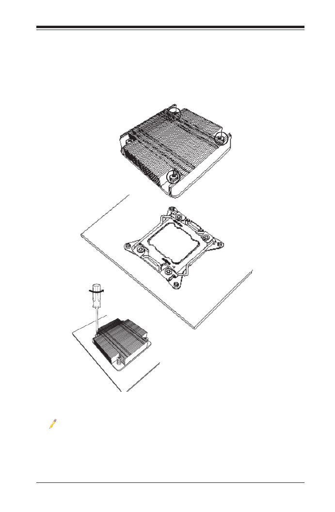
Installing a CPU Heatsink
1. Apply the proper amount of thermal grease to the heatsink.
2. Place the heatsink on top of the CPU so that the two mount-
ing holes on the heatsink are aligned with those on the retention
mechanism.
Note: Graphic drawings included in this manual are for reference
only. They might look different from the components installed in
your system.
Screw#1
Screw#3
Screw#4
Screw#2

2-8
Supermicro C7X99-OCE/C7X99-OCE-F Motherboard User’s Manual
Removing a Heatsink
Warning: We do not recommend that the CPU or the heatsink be removed.
However, if you do need to remove the heatsink, please follow the instruc-
tions below to uninstall the heatsink to avoid damaging the CPU or other
components.
1. Unplug the power cord from the power supply.
2. Loosen the screws.
3. Gently wriggle the heatsink to loosen it. (Do not use excessive
force when wriggling the heatsink.)
4. Once the heatsink is loosened, remove it from the motherboard.

Chapter 2: Installation
2-9
MAC CODE
IPMI CODE
BAR CODE
C7X99-OCE-F
SW_BIOSRC
S4
S7
S10
S5
S6
S9
OC_FRONT_PANEL
S8
S11
CLR_CMOS_SW
JUSB30_I2
JAUDIO1
LED4
I-SATA0I-SATA2I-SATA4S-SATA0S-SATA2
AUDIO_FP
JIPMB1
JSD1
MH11
MH2
MH9
MH10
JPW2
CA
LEDM1
JBT1
BT1
+
FAN5
FAN4
FAN1
1
FAN2
4
FAN3
JPL2
JPUSB1
J29
J30
JPME2
JPAC1
JPL1
JI2C1JI2C2
JPB1
JPG1
JWD11
JL2
JL1
JD1
1
JF1
2
19
JPI2C1
JSTBY1
JTPM1
SP1
+
HD AUDIO
VGA
LAN1
LAN2
USB 16/17(3.0)
USB 12/13(3.0) USB 10/11(3.0)
USB 14/15(3.0)
CPU SLOT6 PCI-E 3.0 X16
PCH SLOT5 PCI-E 2.0 X1 (IN X4)
CPU SLOT4 PCI-E 3.0 X8 (IN X16)
PCH SLOT3 PCI-E 2.0 X1 (IN X4)
CPU SLOT2 PCI-E 3.0 X8 (IN X16)
CPU SLOT1 PCI-E 3.0 X8 (IN X16)
2-3:DISABLE1-2:ENABLE
:WATCH DOG
SPEAKER
PWR LED
:TPM/PORT80
CPU
CHASSIS INTRUSION
JI2C2
2-3:DISABLE1-2:ENABLE
JI2C1
PWR ON OH/FF NIC1NIC2RST X
CMOS CLEAR
1-2:NORMAL
2-3:BIOS RECOVERY
JBR1
PWR LEDHDD LED NMIX
2-3:ME MANUFACTURING MODE
JPME21-2:NORMAL
1-2 ENABLE
2-3 DISABLE
1-2 ENABLE
2-3 DISABLE
:PWR I2C
1-2 ENABLE2-3 DISABLE
2-3 DISABLE
1-2 ENABLE
1-2 ENABLE
2-3 DISABLE
JPAC1
VGA
USB14/15 WAKE UP
1-2 RST2-3 NMI
:SATA DOM POWER
DIMMD2
DIMMD1
DIMMC2
DIMMC1
DIMMB2
DIMMB1
DIMMA2
DIMMA1
JBR1
JWD1
JPW1
JPUSB1
JPB1
JPG1
C
A
LED1
I-SATA1I-SATA3I-SATA5S-SATA1S-SATA3
C7X99-OCE/
COM1
2-4 Installing DDR4 Memory
Note: Check the Supermicro website for recommended memory
modules.
Attention! Exercise extreme care when installing or removing
DIMM modules to prevent any possible damage.
DIMM Installation
1. Insert the desired number of
DIMMs into the memory slots,
starting with DIMMA1 (see the
next page for the location). For
the system to work properly,
please use the memory modules
of the same type and speed in
the same motherboard.
Release Tabs
Notches
2. Push the release tabs outwards
on both ends of the DIMM slot
to unlock it.
Press both notches
straight down into
the memory slot.
3. Align the key of the DIMM mod-
ule with the receptive point on the
memory slot.
4. Align the notches on both ends of
the module against the receptive
points on the ends of the slot.
5. Use two thumbs together to press
the notches on both ends of the
module straight down into the slot
until the module snaps into place.
6. Press the release tabs to the lock
positions to secure the DIMM mod-
ule into the slot.
Removing Memory Modules
Reverse the steps above to remove the
DIMM modules from the motherboard.

2-10
Supermicro C7X99-OCE/C7X99-OCE-F Motherboard User’s Manual
Memory Support
Memory Population Guidelines
When installing memory modules, the DIMM slots should be populated in
the following order: DIMMA1, DIMMB1, DIMMC1, DIMMD1 then DIMMA2,
DIMMB2, DIMMC2, DIMMD2.
• Always use DDR4 DIMM modules of the same size, type and speed.
Recommended Population (Balanced)
DIMMA1 DIMMB1 DIMMC1 DIMMD1 DIMMA2 DIMMB2 DIMMC2 DIMMD2 Total System
Memory
4GB 4GB 8GB
4GB 4GB 4GB 4GB 16GB
4GB 4GB 4GB 4GB 4GB 4GB 24GB
4GB 4GB 4GB 4GB 4GB 4GB 4GB 4GB 32GB
8GB 8GB 16GB
8GB 8GB 8GB 8GB 32GB
8GB 8GB 8GB 8GB 8GB 8GB 48GB
8GB 8GB 8GB 8GB 8GB 8GB 8GB 8GB 64GB
The C7X99-OCE(-F) supports up to 64GB of Unbuffered (UDIMM) DDR4
non-ECC 2133~3300(OC) MHz in 8 memory slots. Populating these
DIMM modules with a pair of memory modules of the same type and
same size will result in interleaved memory, which will improve memory
performance.
Note: For memory optimization, use only DIMM modules that have been
validated by Supermicro. For the latest memory updates, please refer
to our website at http://www.supermicro.com/products/motherboard.
CPU
DIMMB2
DIMMA2
DIMMA1 (Blue Slot)
DIMMB1 (Blue Slot)
DIMMC1 (Blue Slot)
DIMMD1 (Blue Slot)
DIMMD2
DIMMC2
I/O Back Panel

Chapter 2: Installation
2-11
Notes
Be sure to use memory modules of the same type, same speed,
same frequency on the same motherboard. Mixing of memory
modules of different types and speeds is not allowed.
Due to memory allocation to system devices, the amount of
memory that remains available for operational use will be re-
duced when 4 GB of RAM is used. The reduction in memory
availability is disproportional. See the following table for details.
For Microsoft Windows users: Microsoft implemented a design
change in the Windows XP with Service Pack 2 (SP2) and Win-
dows Vista. This change is specic to the behavior of Physical
Address Extension (PAE) mode which improves driver compat-
ibility. For more information, please read the following article at
Microsoft’s Knowledge Base website at: http://support.microsoft.
com/kb/888137.
Possible System Memory Allocation & Availability
System Device Size Physical Memory
Remaining (-Available)
(4 GB Total System
Memory)
Firmware Hub ash memory (System BIOS) 1 MB 3.99
Local APIC 4 KB 3.99
Area Reserved for the chipset 2 MB 3.99
I/O APIC (4 Kbytes) 4 KB 3.99
PCI Enumeration Area 1 256 MB 3.76
PCI Express (256 MB) 256 MB 3.51
PCI Enumeration Area 2 (if needed) -Aligned on 256-MB
boundary-
512 MB 3.01
VGA Memory 16 MB 2.85
TSEG 1 MB 2.84
Memory available to OS and other applications 2.84

2-12
Supermicro C7X99-OCE/C7X99-OCE-F Motherboard User’s Manual
MAC CODE
IPMI CODE
BAR CODE
C7X99-OCE-F
SW_BIOSRC
S4
S7
S10
S5
S6
S9
OC_FRONT_PANEL
S8
S11
CLR_CMOS_SW
JUSB30_I2
JAUDIO1
LED4
I-SATA0I-SATA2I-SATA4S-SATA0
S-SATA2
AUDIO_FP
JIPMB1
JSD1
MH11
MH2
MH9
MH10
JPW2
CA
LEDM1
JBT1
BT1
+
FAN5
FAN4
FAN1
1
FAN2
4
FAN3
JPL2
JPUSB1
J29
J30
JPME2
JPAC1
JPL1
JI2C1
JI2C2
JPB1
JPG1
JWD1
1
JL2
JL1
JD1
1
JF1
2
19
JPI2C1
JSTBY1
JTPM1
SP1
+
HD AUDIO
VGA
LAN1
LAN2
USB 16/17(3.0)
USB 12/13(3.0) USB 10/11(3.0)
USB 14/15(3.0)
CPU SLOT6 PCI-E 3.0 X16
PCH SLOT5 PCI-E 2.0 X1 (IN X4)
CPU SLOT4 PCI-E 3.0 X8 (IN X16)
PCH SLOT3 PCI-E 2.0 X1 (IN X4)
CPU SLOT2 PCI-E 3.0 X8 (IN X16)
CPU SLOT1 PCI-E 3.0 X8 (IN X16)
2-3:DISABLE
1-2:ENABLE
:WATCH DOG
SPEAKERPWR LED
:TPM/PORT80
CPU
CHASSIS INTRUSION
JI2C2
2-3:DISABLE
1-2:ENABLEJI2C1
PWR ON OH/FF NIC1NIC2RST X
CMOS CLEAR
1-2:NORMAL
2-3:BIOS RECOVERY
JBR1
PWR LEDHDD LED NMIX
2-3:ME MANUFACTURING MODE
JPME2
1-2:NORMAL
1-2 ENABLE
2-3 DISABLE
1-2 ENABLE
2-3 DISABLE
:PWR I2C
1-2 ENABLE2-3 DISABLE
2-3 DISABLE
1-2 ENABLE
1-2 ENABLE
2-3 DISABLE
JPAC1
VGA
USB14/15 WAKE UP
1-2 RST
2-3 NMI
:SATA DOM POWER
DIMMD2
DIMMD1
DIMMC2
DIMMC1
DIMMB2
DIMMB1
DIMMA2
DIMMA1
JBR1
JWD1
JPW1
JPUSB1
JPB1
JPG1
C
A
LED1
I-SATA1
I-SATA3
I-SATA5S-SATA1S-SATA3
C7X99-OCE/
COM1
Location of Mounting Holes
Attention! 1) To avoid damaging the motherboard and its com-
ponents, please do not use a force greater than 8 lb/inch on each
mounting screw during motherboard installation. 2) Some compo-
nents are very close to the mounting holes. Please take precautionary
measures to avoid damaging these components when installing the
motherboard to the chassis.
2-5 Motherboard Installation
All motherboards have standard mounting holes to t different types of
chassis. Make sure that the locations of all the mounting holes for both
motherboard and chassis match. Although a chassis may have both plas-
tic and metal mounting fasteners, metal ones are highly recommended
because they ground the motherboard to the chassis. Make sure that the
metal standoffs click in or are screwed in tightly. Then use a screwdriver
to secure the motherboard onto the motherboard tray.
Philips Screwdriver
(1)
Standoffs (9)
Only if Needed
Philips Screws (9)
Tools Needed

Chapter 2: Installation
2-13
Installing the Motherboard
1. Install the I/O shield into the back of the chassis.
2. Locate the mounting holes on the motherboard. (See the previous
page.)
3. Locate the matching mounting holes on the chassis. Align the
mounting holes on the motherboard against the mounting holes on
the chassis.
4. Install standoffs in the chassis as needed.
5. Install the motherboard into the chassis carefully to avoid damaging
other motherboard components.
6. Using the Phillips screwdriver, insert a Phillips head #6 screw into a
mounting hole on the motherboard and its matching mounting hole
on the chassis.
7. Repeat Step 5 to insert #6 screws into all mounting holes.
8. Make sure that the motherboard is securely placed in the chassis.
Note: Images displayed are is for illustration only. Your chassis
or components might look different from those shown in this
manual.
2-14
Supermicro C7X99-OCE/C7X99-OCE-F Motherboard User’s Manual
MAC CODE
IPMI CODE
BAR CODE
C7X99-OCE-F
SW_BIOSRC
S4
S7
S10
S5
S6
S9
OC_FRONT_PANEL
S8
S11
CLR_CMOS_SW
JUSB30_I2
JAUDIO1
LED4
I-SATA0
I-SATA2
I-SATA4S-SATA0S-SATA2
AUDIO_FP
JIPMB1
JSD1
MH11
MH2
MH9
MH10
JPW2
CA
LEDM1
JBT1
BT1
+
FAN5
FAN4
FAN1
1
FAN2
4
FAN3
JPL2
JPUSB1
J29
J30
JPME2
JPAC1
JPL1
JI2C1
JI2C2
JPB1
JPG1
JWD1
1
JL2
JL1
JD1
1
JF1
2
19
JPI2C1
JSTBY1
JTPM1
SP1
+
HD AUDIO
VGA
LAN1
LAN2
USB 16/17(3.0)
USB 12/13(3.0) USB 10/11(3.0)
USB 14/15(3.0)
CPU SLOT6 PCI-E 3.0 X16
PCH SLOT5 PCI-E 2.0 X1 (IN X4)
CPU SLOT4 PCI-E 3.0 X8 (IN X16)
PCH SLOT3 PCI-E 2.0 X1 (IN X4)
CPU SLOT2 PCI-E 3.0 X8 (IN X16)
CPU SLOT1 PCI-E 3.0 X8 (IN X16)
2-3:DISABLE
1-2:ENABLE
:WATCH DOG
SPEAKERPWR LED
:TPM/PORT80
CPU
CHASSIS INTRUSION
JI2C2
2-3:DISABLE
1-2:ENABLEJI2C1
PWR ON OH/FF NIC1NIC2RST X
CMOS CLEAR
1-2:NORMAL
2-3:BIOS RECOVERY
JBR1
PWR LEDHDD LED NMIX
2-3:ME MANUFACTURING MODE
JPME2
1-2:NORMAL
1-2 ENABLE
2-3 DISABLE
1-2 ENABLE
2-3 DISABLE
:PWR I2C
1-2 ENABLE2-3 DISABLE
2-3 DISABLE
1-2 ENABLE
1-2 ENABLE
2-3 DISABLE
JPAC1
VGA
USB14/15 WAKE UP
1-2 RST
2-3 NMI
:SATA DOM POWER
DIMMD2
DIMMD1
DIMMC2
DIMMC1
DIMMB2
DIMMB1
DIMMA2
DIMMA1
JBR1
JWD1
JPW1
JPUSB1
JPB1
JPG1
C
A
LED1
I-SATA1I-SATA3I-SATA5S-SATA1
S-SATA3
C7X99-OCE/
COM1
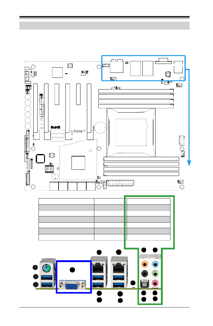
2-6 Connectors/IO Ports
The I/O ports are color coded in conformance with the PC 99 specication.
See the gure below for the colors and locations of the various I/O ports.
Back I/O Panel
A. PS/2 Keyboard/Mouse Port L. Center/LFE OutH. Gb LAN Port 2
B. USB 3.0 Port 14 I. USB 3.0 Port 12 M. Surround Out
C. USB 3.0 Port 15 N. S/PDIF OutJ. USB 3.0 Port 13
D. VGA Port* K. Clear CMOS O. Line In
E. Gb LAN Port 1 (shared IPMI*) P. Line Out
F. USB 3.0 Port 10 Q. Mic In
G. USB 3.0 Port 11
A
B
C
D
E
F
G
H
I
J
K
L
M
N
O
P
Q
HD Audio
* C7X99-OCE-F only
* C7X99-OCE-F only

Chapter 2: Installation
2-15
MAC CODE
IPMI CODE
BAR CODE
C7X99-OCE-F
SW_BIOSRC
S4
S7
S10
S5
S6
S9
OC_FRONT_PANEL
S8
S11
CLR_CMOS_SW
JUSB30_I2
JAUDIO1
LED4
I-SATA0I-SATA2I-SATA4S-SATA0S-SATA2
AUDIO_FP
JIPMB1
JSD1
MH11
MH2
MH9
MH10
JPW2
CA
LEDM1
JBT1
BT1
+
FAN5
FAN4
FAN1
1
FAN2
4
FAN3
JPL2
JPUSB1
J29
J30
JPME2
JPAC1
JPL1
JI2C1
JI2C2
JPB1
JPG1
JWD11
JL2
JL1
JD1
1
JF1
2
19
JPI2C1
JSTBY1
JTPM1
SP1
+
HD AUDIO
VGA
LAN1LAN2
USB 16/17(3.0)
USB 12/13(3.0) USB 10/11(3.0)
USB 14/15(3.0)
CPU SLOT6 PCI-E 3.0 X16
PCH SLOT5 PCI-E 2.0 X1 (IN X4)
CPU SLOT4 PCI-E 3.0 X8 (IN X16)
PCH SLOT3 PCI-E 2.0 X1 (IN X4)
CPU SLOT2 PCI-E 3.0 X8 (IN X16)
CPU SLOT1 PCI-E 3.0 X8 (IN X16)
2-3:DISABLE1-2:ENABLE
:WATCH DOG
SPEAKER
PWR LED
:TPM/PORT80
CPU
CHASSIS INTRUSION
JI2C2
2-3:DISABLE1-2:ENABLE
JI2C1
PWR ON OH/FF NIC1NIC2RST X
CMOS CLEAR
1-2:NORMAL
2-3:BIOS RECOVERY
JBR1
PWR LEDHDD LED NMIX
2-3:ME MANUFACTURING MODE
JPME21-2:NORMAL
1-2 ENABLE
2-3 DISABLE
1-2 ENABLE
2-3 DISABLE
:PWR I2C
1-2 ENABLE2-3 DISABLE
2-3 DISABLE1-2 ENABLE
1-2 ENABLE
2-3 DISABLE
JPAC1
VGA
USB14/15 WAKE UP
1-2 RST2-3 NMI
:SATA DOM POWER
DIMMD2
DIMMD1
DIMMC2
DIMMC1
DIMMB2
DIMMB1
DIMMA2
DIMMA1
JBR1
JWD1
JPW1
JPUSB1
JPB1
JPG1
C
A
LED1
I-SATA1I-SATA3I-SATA5S-SATA1S-SATA3
C7X99-OCE/
COM1
A. Backpanel USB 3.0 #14
B. Backpanel USB 3.0 #15
C. Backpanel USB 3.0 #10
D. Backpanel USB 3.0 #11
E. Backpanel USB 3.0 #12
F. Backpanel USB 3.0 #13
G. USB 3.0 Header #16/17
Universal Serial Bus (USB)
Six USB 3.0 ports (10/11, 12/13, 14/15) are located on the I/O back
panel. In addition, one USB 3.0 header (USB 16/17) is also located on
the motherboard to provide front chassis access using USB cables (not
included). These ports are backward compatible with the USB 2.0 stan-
dard. See the tables below for pin denitions.
Back Panel USB (2.0) #0/1, USB (3.0) #2/3,
12/13 Pin Denitions
Pin# Denition Pin# Denition
1 +5V 5 +5V
2 USB_PN1 6 USB_PN0
3 USB_PP1 7 USB_PP0
4 8Ground Ground
A
Front Panel USB (3.0) Header #14/15
Pin Denitions
Pin# Pin# Signal Name Description
1 10 VBUS Power
2 11 D- USB 2.0 Differential Pair
3 12 D+
4 13 Ground Ground of PWR Return
5 14 StdA_SSRX- SuperSpeed Receiver
6 15 StdA_SSRX+ Differential Pair
7 16 GND_DRAIN Ground for Signal Return
8 17 StdA_SSTX- SuperSpeed Transmitter
9 18 StdA_SSTX+ Differential Pair
CE
B
F
D
G
2-16
Supermicro C7X99-OCE/C7X99-OCE-F Motherboard User’s Manual
Ethernet Ports
Two Gigabit Ethernet ports (LAN1/LAN2)
are located next to the HD Audio Con-
nector on the I/O Backpanel to provide
network connections. These ports accept
RJ45 type cables.
Note: Please refer to the LED Indica-
tor Section for LAN LED information.
LAN Ports
Pin Definition
Pin# Denition Pin# Denition
1 P2V5SB 10 SGND
2 TD0+ 11 Act LED
3 12 P3V3SBTD0-
4 13TD1+ Link 100 LED
(Green, +3V3SB)
5 14TD1- Link 1000 LED
(Yellow, +3V3SB)
6 15TD2+ Ground
7 16TD2- Ground
8 17TD3+ Ground
9 88TD3- Ground
(NC: No Connection)
A. LAN1
B. LAN2
C. Center/LFE Out
D. Surround Out
E. S/PDIF Out
F. Line In
G. Line Out
H. Mic In
Back Panel High Denition Audio
(HD Audio)
This motherboard features a 5.1+2
Channel High Denition Audio (HDA) co-
dec that provides 10 DAC channels. The
HD Audio connections simultaneously
supports multiple-streaming 5.1 sound
playback with 2 channels of independent
stereo output through the front panel
stereo out for front, rear, center and
subwoofer speakers. Use the Advanced
software included in the CD-ROM with
your motherboard to enable this func-
tion.
A
E
B
F
G
C
D
H

2-18
Supermicro C7X99-OCE/C7X99-OCE-F Motherboard User’s Manual
C7X99-OCE-F
S11
JUSB30_I2
MH2
1
4
1
1
19
Front Control Panel
JF1 contains header pins for various buttons and indicators that are
normally located on a control panel at the front of the chassis. These
connectors are designed specically for use with Supermicro chassis. See
the gure below for the descriptions of the front control panel buttons
and LED indicators. Refer to the following section for descriptions and
pin denitions.
Pin 19Pin 20
Pin 1
Pin 2
JF1 Header Pins
Power Button
OH/Fan Fail LED
1
NIC1 LED
Reset Button
2
Power Fail LED
HDD LED
Power LED
#3~4
#1~2
Vcc
Vcc
Vcc
Vcc
Ground
Ground
1920
Vcc
X
Ground NMI
X
Vcc
NIC2 LED

Chapter 2: Installation
2-19
Power Button
OH/Fan Fail LED
1
NIC1 LED
Reset Button
2
Power Fail LED
HDD LED
Power LED
#3~4
#1~2
Vcc
Vcc
Vcc
Vcc
Ground
Ground
1920
Vcc
X
Ground NMI
X
Vcc
NIC2 LED
Front Control Panel Pin Definitions
Power LED
The Power LED connection is located on
pins 15 and 16 of JF1. Refer to the table
on the right for pin denitions.
Power LED
Pin Denitions (JF1)
Pin# Denition
15 +3.3V
16 Ground
A. PWR LED
B. HDD LED
A
B
HDD LED
The HDD LED connection is located on
pins 13 and 14 of JF1. Attach a cable
here to indicate the status of HDD-
related activities, including IDE, SATA
activities. See the table on the right for
pin denitions.
HDD LED
Pin Denitions (JF1)
Pin# Denition
13 +3.3V
14 HD Active
NIC1/NIC2 (LAN1/LAN2)
The NIC (Network Interface Controller)
LED connection for LAN port 1 is located
on pins 11 and 12 of JF1, and the LED
connection for LAN Port 2 is on Pins 9
and 10. NIC1 LED and NIC2 LED are
2-pin NIC LED headers. Attach NIC LED
cables to NIC1 and NIC2 LED indicators
to display network activities. Refer to
the table on the right for pin denitions.
LAN1/LAN2 LED
Pin Denitions (JF1)
Pin# Denition
9/11 Vcc
10/12 Ground
Overheat (OH)/Fan Fail
Connect an LED cable to OH/Fan Fail
connections on pins 7 and 8 of JF1 to
provide warnings for chassis overheat/
fan failure. Refer to the table on the right
for pin denitions.
OH/Fan Fail LED
Pin Denitions (JF1)
Pin# Denition
7 Vcc
8OH/Fan Fail LED
OH/Fan Fail Indicator
Status
State Denition
Off Normal
On Overheat
Flash-
ing
Fan Fail
C. NIC1 LED
D. NIC2 LED
E. OH/Fan Fail
C
D
E
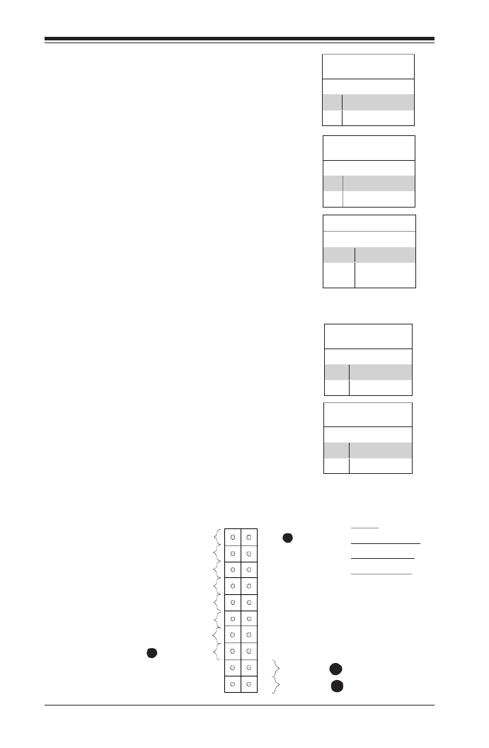
2-20
Supermicro C7X99-OCE/C7X99-OCE-F Motherboard User’s Manual
Power Button
The Power Button connection is located
on pins1 and 2 of JF1. Momentarily
contacting both pins will power on/off
the system. This button can also be con-
gured to function as a suspend button
(with a setting in the BIOS - see Chapter
4). To turn off the power in the suspend
mode, press the button for at least 4
seconds. Refer to the table on the right
for pin denitions.
Power Button
Pin Denitions (JF1)
Pin# Denition
1Signal
2+3V Standby
Reset Button
The Reset Button connection is located
on pins 3 and 4 of JF1. Attach it to a
hardware reset switch on the computer
case to reset the system. Refer to the
table on the right for pin denitions. Reset Button
Pin Denitions (JF1)
Pin# Denition
3Reset
4Ground
A. NMI
B. PWR Fail LED
C. Reset Button
D. PWR Button
Power Button
OH/Fan Fail LED
1
NIC1 LED
Reset Button
2
Power Fail LED
HDD LED
Power LED
#3~4
#1~2
Vcc
Vcc
Vcc
Vcc
Ground
Ground
1920
Vcc
X
Ground NMI
X
Vcc
NIC2 LED
A
B
C
D
NMI Button
The non-maskable interrupt button-
header is located on pins 19 and 20 of
JF1. Refer to the table on the rightfor
pin denitions.
Power Fail
Connect an LED cable to the Power Fail
connection to provide a warning that a
power failure has occured. Refer to the
table on the right for pin denitions.
Power Fail LED
Pin Denitions (JF1)
Pin# Denition
5 Vcc
6Power Fail LED
Power Fail LED Status
State Denition
Off Normal
Flash-
ing
Power Fail
NMI
Pin Denitions (JF1)
Pin# Denition
19 NMI
20 Ground

Chapter 2: Installation
2-21
MAC CODE
IPMI CODE
BAR CODE
C7X99-OCE-F
SW_BIOS RC
S4
S7
S10
S5
S6
S9
OC_FRONT_PA NEL
S8
S11
CLR_CMOS_SW
JUSB30_I2
JAUDIO1
LED 4
I-SATA0I-SATA2I-SATA4S-SATA0S-SATA2
AUDIO_FP
JIPMB1
JSD1
MH11
MH2
MH9
MH10
JPW2
CA
LEDM1
JBT1
BT1
+
FAN5
FAN4
FAN1
1
FAN2
4
FAN3
JPL2
JPUSB1
J29
J30
JPME2
JPAC1
JPL1
JI2C1
JI2C2
JPB1
JPG1
JWD11
JL2
JL1
JD1
1
JF1
2
19
JPI2C1
JSTBY1
JTPM1
SP1
+
HD AUDIO
VGA
LAN 1
LAN 2
USB 16/17(3.0)
USB 12/13(3.0) USB 10/11(3.0)
USB 14/15(3.0)
CPU SLOT6 PCI-E 3.0 X16
PCH SL OT5 PCI-E 2.0 X1 (IN X4)
CPU SLOT4 PCI-E 3.0 X8 (IN X16)
PCH SL OT3 PCI-E 2.0 X1 (IN X4)
CPU SLOT2 PCI-E 3.0 X8 (IN X16)
CPU SLOT1 PCI-E 3.0 X8 (IN X16)
2-3:DISABLE1-2 :ENABLE
:WATCH DOG
SPEAKER
PWR LED
:TPM/PORT80
CPU
CHASSIS INTRUSION
JI2C2
2-3:DISABLE1-2 :ENABLE
JI2C1
PWR ON OH/FF NIC1NIC2RST X
CMOS CLEAR
1-2:NORMAL
2-3:BIOS RECOVERY
JBR1
PWR LEDHDD LED NMIX
2-3:ME MANUFACTURING MODE
JPME2
1-2:NORMAL
1-2 ENABLE
2-3 DISABLE
1-2 ENABLE
2-3 DISABLE
:PWR I2C
1-2 ENABLE2-3 DISABLE
2-3 DISABLE
1-2 ENABLE
1-2 ENABLE
2-3 DISABLE
JPAC1
VGA
USB14/15 WAKE UP
1-2 RST
2-3 NMI
:SATA DOM POWER
DIM MD 2
DIM MD 1
DIM MC2
DIM MC1
DIM MB 2
DIM MB 1
DIM MA2
DIM MA1
JBR1
JWD1
JPW1
JPUSB1
JPB1
JPG1
C
A
LED1
I-SATA1I-SATA3I-SATA5S-SATA1
S-SATA3
C7X99-OCE/
COM1
2-7 Connecting Cables
This section provides brief descriptions and pin-out denitions for on-
board headers and connectors. Be sure to use the correct cable for each
header or connector.
A. 24-Pin ATX Main PWR
B. 8-Pin PWR
ATX Power 24-pin Connector
Pin Denitions (JPW1)
Pin# Denition Pin # Denition
13 +3.3V 1 +3.3V
14 2 +3.3V-12V
15 3COM COM
16 4 +5VPS_ON
17 5COM COM
18 6 +5VCOM
19 7COM COM
20 8Res (NC) PWR_OK
21 +5V 9 5VSB
22 +5V 10 +12V
23 +5V +12V11
24 12 +3.3VCOM
(Required)
12V 8-pin Power Connec-
tor Pin Denitions
Pins Denition
1 through 4 Ground
5 through 8 +12V
ATX Main PWR & CPU PWR
Connectors (JPW1 & JPW2)
The 24-pin main power connector (JPW1)
is used to provide power to the moth-
erboard. The 8-pin CPU PWR connector
(JPW2) is also required for the processor.
These power connectors meet the SSI
EPS 12V specication. See the table on
the right for pin denitions.
A
B
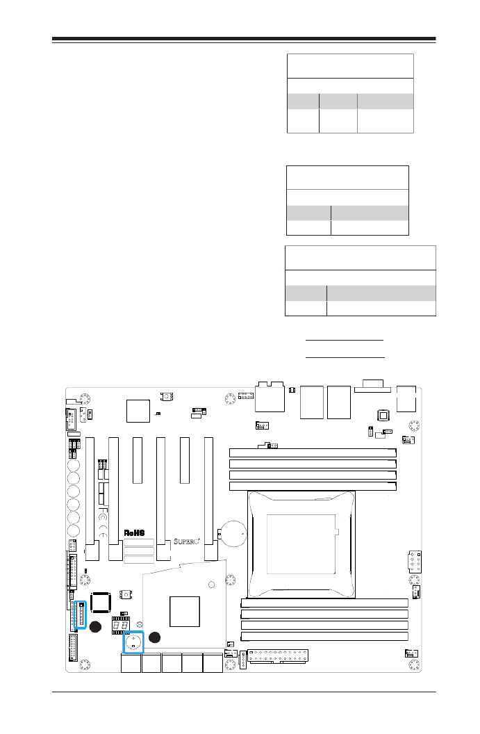
Chapter 2: Installation
2-23
Internal Buzzer (SP1)
The Internal Buzzer (SP1) can be used
to provide audible indications for various
beep codes. See the table on the right
for pin denitions. See JD1 description
below for jumper settings.
A. Internal Buzzer
B. Speaker Header
Internal Buzzer
Pin Denition
Pin# Denitions
Pin 1 Pos. (+) Beep In
Pin 2 Neg. (-) Alarm
Speaker
Power LED / Speaker (JD1)
On the JD1 header, pins 1~3 are used
to connect to the Power LED indicator
on the chassis. Use pins 4-7 to connect
to an external speaker. If the onboard
Buzzer/Speaker (SP1) is required in-
stead, please close/short pins 6~7 with
a jumper (default). See the table on
the right for pin denitions and settings.
Power LED/Speaker Connector
Pin Denitions
Pin# Denition
Pins 4-7 External Speaker
Pins 1~3 Power LED
MAC CODE
IPMI CODE
BAR CODE
C7X99-OCE-F
SW_BIOSRC
S4
S7
S10
S5
S6
S9
OC_FRONT _PANEL
S8
S11
CLR _CMO S_SW
JUSB30_I2
JAUDIO1
LED4
I-SATA0I-SATA2I-SATA4S-SATA0
S-SATA2
AUDIO_F P
JIPM B1
JSD1
MH11
MH2
MH9
MH10
JPW2
CA
LED M1
JBT1
BT1
+
FAN5
FAN4
FAN1
1
FAN2
4
FAN3
JPL2
JPUSB1
J29
J30
JPME 2
JPAC1
JPL1
JI2C1
JI2C2
JPB1
JPG1
JWD1
1
JL2
JL1
JD1
1
JF1
2
19
JPI2C 1
JSTBY1
JTPM1
SP1
+
HD AUDIO
VGA
LAN1
LAN2
USB 16/17(3.0)
USB 12/13(3.0) USB 10/11(3.0)
USB 14/15(3.0)
CPU SLOT6 PCI-E 3.0 X16
PCH SLOT5 PCI-E 2.0 X1 (IN X4)
CPU SLOT4 PCI-E 3.0 X8 (IN X16)
PCH SLOT3 PCI-E 2.0 X1 (IN X4)
CPU SLOT2 PCI-E 3.0 X8 (IN X16)
CPU SLOT1 PCI-E 3.0 X8 (IN X16)
2-3:DISABLE
1-2:ENABLE
:WATCH DOG
SPEAKERPWR LED
:TPM/PORT80
CPU
CHASSIS I NTRUSION
JI2C2
2-3:DISABLE
1-2:ENABLEJI2C1
PWR ON OH/FF NIC1NIC2RST X
CMOS CLEAR
1-2:NORMAL
2-3:BIOS RECOVERY
JBR1
PWR LEDHDD LED NMIX
2-3:ME MANUFACTURING MODE
JPME2
1-2:NORMAL
1-2 ENABLE
2-3 DISABLE
1-2 ENABLE
2-3 DISABLE
:PWR I2C
1-2 ENABLE2-3 DISABLE
2-3 DISABLE
1-2 ENABLE
1-2 ENABLE
2-3 DISABLE
JPAC1
VGA
USB14/15 WAKE UP
1-2 RST
2-3 NMI
:SATA DOM POWER
DIMMD2
DIMMD1
DIMMC2
DIMMC1
DIMMB2
DIMMB1
DIMMA2
DIMMA1
JBR1
JWD1
JPW1
JPUSB1
JPB1
JPG1
C
A
LED 1
I-SATA1
I-SATA3
I-SATA5S-SATA1S-SATA3
C7X99-OCE/
COM1
A
B
Speaker Connector
Jumper Settings
Pin Setting Denition
Pins 6-7 Closed (Onboard Speaker)l
Pins 6~7 Open (External Speaker)

2-24
Supermicro C7X99-OCE/C7X99-OCE-F Motherboard User’s Manual
DOM PWR Connector (JSD1)
The Disk-On-Module (DOM) power con-
nector, located at JSD1, provides 5V
(Gen1/Gen) power to a solid state DOM
storage device connected to one of the
SATA ports. See the table on the right
for pin denitions.
DOM PWR
Pin Denitions
Pin# Denition
1 5V
2Ground
3Ground
MAC CODE
IPMI CODE
BAR CODE
C7X99-OCE-F
SW_BIOSRC
S4
S7
S10
S5
S6
S9
OC_FRON T_PANEL
S8
S11
CLR_CMOS_SW
JUSB30_I2
JAUDIO1
LED4
I-SATA0I-SATA2I-SATA4S-SATA0S-SATA2
AUDIO_FP
JIPMB1
JSD1
MH11
MH2
MH9
MH10
JPW2
CA
LEDM 1
JBT1
BT1
+
FAN5
FAN4
FAN1
1
FAN2
4
FAN3
JPL2
JPUSB1
J29
J30
JPME2
JPAC1
JPL1
JI2C1
JI2C2
JPB1
JPG1
JWD1
1
JL2
JL1
JD1
1
JF1
2
19
JPI2C1
JSTBY1
JTPM1
SP1
+
HD AUDIO
VGA
LAN1
LAN2
USB 16/17(3.0)
USB 12/13(3.0) USB 10/11(3.0)
USB 14/15(3.0)
CPU SLOT6 PCI-E 3.0 X16
PCH SLOT5 PCI-E 2.0 X1 (IN X4)
CPU SLOT4 PCI-E 3.0 X8 (IN X16)
PCH SLOT3 PCI-E 2.0 X1 (IN X4)
CPU SLOT2 PCI-E 3.0 X8 (IN X16)
CPU SLOT1 PCI-E 3.0 X8 (IN X16)
2-3:DISABLE
1-2:ENABLE
:WATCH DOG
SPEAKERPWR LED
:TPM/PORT80
CPU
CHASSI S IN TRUSION
JI2C2
2-3:DISABLE
1-2:ENABLEJI2C1
PWR ON OH/FF NIC1NIC2RST X
CMOS CLEAR
1-2:NORMAL
2-3:BIOS RECOVERY
JBR1
PWR LEDHDD LED NMIX
2-3:ME MANUFACTURING MODE
JPME2
1-2:NORMAL
1-2 ENABLE
2-3 DISABLE
1-2 ENABLE
2-3 DISABLE
:PWR I2C
1-2 ENABLE2-3 DISABLE
2-3 DISABLE
1-2 ENABLE
1-2 ENABLE
2-3 DISABLE
JPAC1
VGA
USB14/15 WAKE UP
1-2 RST
2-3 NMI
:SATA DOM POWER
DIMMD2
DIMMD1
DIMMC2
DIMMC1
DIMMB2
DIMMB1
DIMMA2
DIMMA1
JBR1
JWD1
JPW1
JPUSB1
JPB1
JPG1
C
A
LED1
I-SATA1
I-SATA3
I-SATA5S-SATA1S-SATA3
C7X99-OCE/
COM1
A
B
A. DOM Power
B STBY PWR
C System Management Bus
Standby Power Header (STBY1)
The Standby Power header is located
at STBY1 on the motherboard. See the
table on the right for pin denitions.
Standby Power
Pin Denitions
Pin# Denition
1+5V Standby
2Ground
3Wake-up
System Management Bus (JIPMB1)
A System Management Bus header for the
IPMI slot is located at IPMB. Connect the
appropriate cable here to use the IPMB
I2C connection on your system. For the
C7X99-OCE-F only.
System Management
Bus
Pin# Denition
1Clock
2Ground
3Data
4No Connection
C

Chapter 2: Installation
2-25
MAC CODE
IPMI CODE
BAR CODE
C7X99-OCE-F
SW_BIOSRC
S4
S7
S10
S5
S6
S9
OC_FRONT _PANEL
S8
S11
CLR _CMO S_SW
JUSB30_I2
JAUDIO1
LED4
I-SATA0I-SATA2I-SATA4S-SATA0
S-SATA2
AUDIO_F P
JIPM B1
JSD1
MH11
MH2
MH9
MH10
JPW2
CA
LED M1
JBT1
BT1
+
FAN5
FAN4
FAN1
1
FAN2
4
FAN3
JPL2
JPUSB1
J29
J30
JPME 2
JPAC1
JPL1
JI2C1
JI2C2
JPB1
JPG1
JWD1
1
JL2
JL1
JD1
1
JF1
2
19
JPI2C 1
JSTBY1
JTPM1
SP1
+
HD AUDIO
VGA
LAN1
LAN2
USB 16/17(3.0)
USB 12/13(3.0) USB 10/11(3.0)
USB 14/15(3.0)
CPU SLOT6 PCI-E 3.0 X16
PCH SLOT5 PCI-E 2.0 X1 (IN X4)
CPU SLOT4 PCI-E 3.0 X8 (IN X16)
PCH SLOT3 PCI-E 2.0 X1 (IN X4)
CPU SLOT2 PCI-E 3.0 X8 (IN X16)
CPU SLOT1 PCI-E 3.0 X8 (IN X16)
2-3:DISABLE
1-2:ENABLE
:WATCH DOG
SPEAKERPWR LED
:TPM/PORT80
CPU
CHASSIS I NTRUSION
JI2C2
2-3:DISABLE
1-2:ENABLEJI2C1
PWR ON OH/FF NIC1NIC2RST X
CMOS CLEAR
1-2:NORMAL
2-3:BIOS RECOVERY
JBR1
PWR LEDHDD LED NMIX
2-3:ME MANUFACTURING MODE
JPME2
1-2:NORMAL
1-2 ENABLE
2-3 DISABLE
1-2 ENABLE
2-3 DISABLE
:PWR I2C
1-2 ENABLE2-3 DISABLE
2-3 DISABLE
1-2 ENABLE
1-2 ENABLE
2-3 DISABLE
JPAC1
VGA
USB14/15 WAKE UP
1-2 RST
2-3 NMI
:SATA DOM POWER
DIMMD2
DIMMD1
DIMMC2
DIMMC1
DIMMB2
DIMMB1
DIMMA2
DIMMA1
JBR1
JWD1
JPW1
JPUSB1
JPB1
JPG1
C
A
LED 1
I-SATA1I-SATA3I-SATA5S-SATA1S-SATA3
C7X99-OCE/
COM1
Trusted Platform Module Header
Pin Denitions
Pin # Denition Pin # Denition
1 2LCLK GND
3 4LFRAME No Pin
5 6LRESET VCC5
7 8LAD3 LAD2
9 10VCC3 LAD1
11 LAD0 GND12
13 14SMBCLK SMBDAT
15 SB3V 16 SERIRQ
17 18GND CLKRUN
19 20LPCPD LDRQ1
TPM Header (JTPM1)
This header is used to connect a
Trusted Platform Module (TPM), which
is available from a third-party vendor.
A TPM is a security device that sup-
ports encryption and authentication
in hard drives. It enables the moth-
erboard to deny access if the TPM
associated with the hard drive is not
installed in the system. See the table
on the right for pin denitions.
Power Supply I2C (JPI2C1)
The Power Supply I2C Connec-
tor, located at JPI2C, monitors
the status of the power supply,
fan and system temperature.
See the table on the right for pin
denitions.
PWR Supply I2C
Pin Denitions
Pin# Denition
1Clock
2Data
3PWR Fail
4 Ground
5 3.3V
A
B
A. TPM Header
B. Power Supply I2C

2-26
Supermicro C7X99-OCE/C7X99-OCE-F Motherboard User’s Manual
MAC CODE
IPMI CODE
BAR CODE
C7X99-OCE-F
SW_BIOSRC
S4
S7
S10
S5
S6
S9
OC_FRONT _PANEL
S8
S11
CLR _CMO S_SW
JUSB30_I2
JAUDIO1
LED4
I-SATA0I-SATA2I-SATA4S-SATA0
S-SATA2
AUDIO_F P
JIPM B1
JSD1
MH11
MH2
MH9
MH10
JPW2
CA
LED M1
JBT1
BT1
+
FAN5
FAN4
FAN1
1
FAN2
4
FAN3
JPL2
JPUSB1
J29
J30
JPME 2
JPAC1
JPL1
JI2C1
JI2C2
JPB1
JPG1
JWD1
1
JL2
JL1
JD1
1
JF1
2
19
JPI2C 1
JSTBY1
JTPM1
SP1
+
HD AUDIO
VGA
LAN1LAN2
USB 16/17(3.0)
USB 12/13(3.0) USB 10/11(3.0)
USB 14/15(3.0)
CPU SLOT6 PCI-E 3.0 X16
PCH SLOT5 PCI-E 2.0 X1 (IN X4)
CPU SLOT4 PCI-E 3.0 X8 (IN X16)
PCH SLOT3 PCI-E 2.0 X1 (IN X4)
CPU SLOT2 PCI-E 3.0 X8 (IN X16)
CPU SLOT1 PCI-E 3.0 X8 (IN X16)
2-3:DISABLE
1-2:ENABLE
:WATCH DOG
SPEAKERPWR LED
:TPM/PORT80
CPU
CHASSIS I NTRUSION
JI2C2
2-3:DISABLE
1-2:ENABLEJI2C1
PWR ON OH/FF NIC1NIC2RST X
CMOS CLEAR
1-2:NORMAL
2-3:BIOS RECOVERY
JBR1
PWR LEDHDD LED NMIX
2-3:ME MANUFACTURING MODE
JPME2
1-2:NORMAL
1-2 ENABLE
2-3 DISABLE
1-2 ENABLE
2-3 DISABLE
:PWR I2C
1-2 ENABLE2-3 DISABLE
2-3 DISABLE
1-2 ENABLE
1-2 ENABLE
2-3 DISABLE
JPAC1
VGA
USB14/15 WAKE UP
1-2 RST
2-3 NMI
:SATA DOM POWER
DIMMD2
DIMMD1
DIMMC2
DIMMC1
DIMMB2
DIMMB1
DIMMA2
DIMMA1
JBR1
JWD1
JPW1
JPUSB1
JPB1
JPG1
C
A
LED 1
I-SATA1I-SATA3I-SATA5S-SATA1S-SATA3
C7X99-OCE/
COM1
A. AUDIO FP
B. OC FRONT PANEL
A
Front Panel Audio Header (AUDIO
FP)
A 10-pin Audio header is supported on
the motherboard. This header allows you
to connect the motherboard to a front
panel audio control panet, if needed.
Connect an audio cable to the audio
header to use this feature (not supplied).
See the table at right for pin denitions
for the header.
10-in Audio
Pin Denitions
Pin# Signal
1Microphone_Left
2Audio_Ground
3Microphone_Right
4Audio_Detect
5Line_2_Right
6Ground
7Jack_Detect
8Key
9Line_2_Left
10 Ground
OC Front Panel (OC FRONT PANEL)
This header is for the Over-Clocking (OC)
control panel which is included with the
motherboard. Attach the control panel's
cable to this header. The OC control panel
enables over-clocking control and man-
agement from the front of the chassis.
See Section 2-10 for more details.
B

Chapter 2: Installation
2-27
2-8 Jumper Settings
Explanation of Jumpers
To modify the operation of the mother-
board, jumpers can be used to choose
between optional settings. Jumpers
create shorts between two pins to
change the function of the connector.
Pin 1 is identied with a square solder
pad on the printed circuit board.
Note: On two pin jumpers, "Closed"
means the jumper is on, and "Open"
means the jumper is off the pins.
A. JPL1: LAN1 Enable
B. JPL2: LAN2 Enable
LAN1/LAN2 Enable/Disable
Jumpers JPL1/JPL2 enable or disable LAN
ports 1/2 on the motherboard. See the
table on the right for jumper settings.
The default setting is enabled.
GLAN Enable
Jumper Settings
Pin# Denition
1-2 Enabled (default)
2-3 Disabled
MAC CODE
IPMI COD E
BAR COD E
C7X99-OCE-F
SW_BIOSRC
S4
S7
S10
S5
S6
S9
OC_FRONT_PANEL
S8
S11
CLR_CMOS_SW
JUSB30_I2
JAUDIO1
LED4
I-SATA0I-SATA2I-SATA4S-SATA0
S-SATA2
AUDIO_FP
JIPMB1
JSD1
MH11
MH2
MH9
MH10
JPW2
CA
LEDM1
JBT1
BT1
+
FAN5
FAN4
FAN1
1
FAN2
4
FAN3
JPL2
JPUSB1
J29
J30
JPME2
JPAC1
JPL1
JI2C1
JI2C2
JPB1
JPG1
JWD1
1
JL2
JL1
JD1
1
JF1
2
19
JPI2C1
JSTBY1
JTPM1
SP1
+
HD AUDIO
VGA
LAN1LAN2
USB 16/17(3.0)
USB 12/13(3.0) USB 10/11(3.0)
USB 14/15(3.0)
CPU SLOT6 PCI-E 3.0 X16
PCH SLOT5 PCI-E 2.0 X1 (IN X4)
CPU SLOT4 PCI-E 3.0 X8 (IN X16)
PCH SLOT3 PCI-E 2.0 X1 (IN X4)
CPU SLOT2 PCI-E 3.0 X8 (IN X16)
CPU SLOT1 PCI-E 3.0 X8 (IN X16)
2-3:DISABLE
1-2:ENABLE
:WATCH DOG
SPEAKERPWR LED
:TPM/PORT80
CPU
CHASSIS INTRUSION
JI2C2
2-3:DISABLE
1-2:ENABLEJI2C1
PWR ON OH/FF NIC1NIC2RSTX
CMOS CLEAR
1-2:NORMAL
2-3:BIOS RECOVERY
JBR1
PWR LEDHDD LED NMIX
2-3:ME MANUFACTURING MODE
JPME2
1-2:NORMAL
1-2 ENABLE
2-3 DISABLE
1-2 ENABLE
2-3 DISABLE
:PWR I2C
1-2 ENABLE2-3 DISABLE
2-3 DISABLE
1-2 ENABLE
1-2 ENABLE
2-3 DISABLE
JPAC1
VGA
USB14/15 WAKE UP
1-2 RST
2-3 NMI
:SATA DOM POWER
DIMMD2
DIMMD1
DIMMC2
DIMMC1
DIMMB2
DIMMB1
DIMMA2
DIMMA1
JBR1
JWD1
JPW1
JPUSB1
JPB1
JPG1
C
A
LED1
I-SATA1I-SATA3I-SATA5S-SATA1
S-SATA3
C7X99-OCE/
COM1
A
B

2-28
Supermicro C7X99-OCE/C7X99-OCE-F Motherboard User’s Manual
Clear CMOS (JBT1, CLR_CMOS_SW)
JBT1 and CLR_CMOS_SW are used to clear the saved system setup con-
guration stored in the CMOS chip. To clear the contents of the CMOS,
completely shut down the system, remove the AC power cord and then
short JBT1 with a jumper or use the push button switch on CLR_CMOS_
SW. Remove the jumper before powering on the system again. This will
erase all user settings and revert everything to their factory-set defaults.
A. Clear CMOS
B. JI2C1
C. JI2C2
D. CLR_CMOS_SW
PCI Slot_SMB Enable
Jumper Settings
Jumper Setting Denition
Short Enabled
Open (Default) Disabled
PCI Slot SMB Enable (I2C1/I2C2)
Use Jumpers I2C1/I2C2 to enable PCI
SMB (System Management Bus) support
to improve system management for the
PCI slots. See the table on the right for
jumper settings.
MAC CODE
IPMI CODE
BAR CODE
C7X99-OCE-F
SW_BIOSRC
S4
S7
S10
S5
S6
S9
OC_FRONT_PANEL
S8
S11
CLR_CMOS_SW
JUSB30_I2
JAUDIO1
LED4
I-SATA0I-SATA2I-SATA4S-SATA0
S-SATA2
AUDIO_FP
JIPMB1
JSD1
MH11
MH2
MH9
MH10
JPW2
CA
LEDM1
JBT1
BT1
+
FAN5
FAN4
FAN1
1
FAN2
4
FAN3
JPL2
JPUSB1
J29
J30
JPME2
JPAC1
JPL1
JI2C1
JI2C2
JPB1
JPG1
JWD1
1
JL2
JL1
JD1
1
JF1
2
19
JPI2C1
JSTBY1
JTPM1
SP1
+
HD AUDIO
VGA
LAN1
LAN2
USB 16/17(3.0)
USB 12/13(3.0) USB 10/11(3.0)
USB 14/15(3.0)
CPU SLOT6 PCI-E 3.0 X16
PCH SLOT5 PCI-E 2.0 X1 (IN X4)
CPU SLOT4 PCI-E 3.0 X8 (IN X16)
PCH SLOT3 PCI-E 2.0 X1 (IN X4)
CPU SLOT2 PCI-E 3.0 X8 (IN X16)
CPU SLOT1 PCI-E 3.0 X8 (IN X16)
2-3:DISABLE
1-2:ENABLE
:WATCH DOG
SPEAKERPWR LED
:TPM/PORT80
CPU
CHASSIS INTRUSION
JI2C2
2-3:DISABLE
1-2:ENABLEJI2C1
PWR ON OH/FF NIC1NIC2RST X
CMOS CLEAR
1-2:NORMAL
2-3:BIOS RECOVERY
JBR1
PWR LEDHDD LED NMIX
2-3:ME MANUFACTURING MODE
JPME2
1-2:NORMAL
1-2 ENABLE
2-3 DISABLE
1-2 ENABLE
2-3 DISABLE
:PWR I2C
1-2 ENABLE2-3 DISABLE
2-3 DISABLE
1-2 ENABLE
1-2 ENABLE
2-3 DISABLE
JPAC1
VGA
USB14/15 WAKE UP
1-2 RST
2-3 NMI
:SATA DOM POWER
DIMMD2
DIMMD1
DIMMC2
DIMMC1
DIMMB2
DIMMB1
DIMMA2
DIMMA1
JBR1
JWD1
JPW1
JPUSB1
JPB1
JPG1
C
A
LED1
I-SATA1I-SATA3I-SATA5S-SATA1
S-SATA3
C7X99-OCE/
COM1
C
A
B
D

Chapter 2: Installation
2-29
A. Audio Enable
B. Watch Dog Enable
Audio Enable/Disable
Jumper Settings
Both Jumpers Denition
Pins 1-2 Enabled
Pins 2-3 Disabled
Audio Enable (JPAC1)
JPAC1 allows you to enable or disable the
onboard audio support. The default posi-
tion is on pins 1 and 2 to enable onboard
audio connections. See the table on the
right for jumper settings.
MAC CODE
IPMI CODE
BAR CODE
C7X99-OCE-F
SW_BIOSRC
S4
S7
S10
S5
S6
S9
OC_FRONT_PANEL
S8
S11
CLR_CMOS_SW
JUSB30_I2
JAUDIO1
LED4
I-SATA0
I-SATA2
I-SATA4S-SATA0S-SATA2
AUDIO_FP
JIPMB1
JSD1
MH11
MH2
MH9
MH10
JPW2
CA
LEDM1
JBT1
BT1
+
FAN5
FAN4
FAN1
1
FAN2
4
FAN3
JPL2
JPUSB1
J29
J30
JPME2
JPAC1
JPL1
JI2C1
JI2C2
JPB1
JPG1
JWD1
1
JL2
JL1
JD1
1
JF1
2
19
JPI2C1
JSTBY1
JTPM1
SP1
+
HD AUDIO
VGA
LAN1
LAN2
USB 16/17(3.0)
USB 12/13(3.0) USB 10/11(3.0)
USB 14/15(3.0)
CPU SLOT6 PCI-E 3.0 X16
PCH SLOT5 PCI-E 2.0 X1 (IN X4)
CPU SLOT4 PCI-E 3.0 X8 (IN X16)
PCH SLOT3 PCI-E 2.0 X1 (IN X4)
CPU SLOT2 PCI-E 3.0 X8 (IN X16)
CPU SLOT1 PCI-E 3.0 X8 (IN X16)
2-3:DISABLE
1-2:ENABLE
:WATCH DOG
SPEAKERPWR LED
:TPM/PORT80
CPU
CHASSIS INTRUSION
JI2C2
2-3:DISABLE
1-2:ENABLEJI2C1
PWR ON OH/FF NIC1NIC2RST X
CMOS CLEAR
1-2:NORMAL
2-3:BIOS RECOVERY
JBR1
PWR LEDHDD LED NMIX
2-3:ME MANUFACTURING MODE
JPME2
1-2:NORMAL
1-2 ENABLE
2-3 DISABLE
1-2 ENABLE
2-3 DISABLE
:PWR I2C
1-2 ENABLE2-3 DISABLE
2-3 DISABLE
1-2 ENABLE
1-2 ENABLE
2-3 DISABLE
JPAC1
VGA
USB14/15 WAKE UP
1-2 RST
2-3 NMI
:SATA DOM POWER
DIMMD2
DIMMD1
DIMMC2
DIMMC1
DIMMB2
DIMMB1
DIMMA2
DIMMA1
JBR1
JWD1
JPW1
JPUSB1
JPB1
JPG1
C
A
LED1
I-SATA1I-SATA3I-SATA5S-SATA1
S-SATA3
C7X99-OCE/
COM1
A
B
Watch Dog Enable/Disable
Watch Dog (JWD1) is a system monitor that
can reboot the system when a software appli-
cation hangs. Close Pins 1-2 to reset the sys-
tem if an application hangs. Close Pins 2-3 to
generate a non-maskable interrupt signal for
the application that hangs. See the table on
the right for jumper settings. Watch Dog must
also be enabled in the BIOS.
Watch Dog
Jumper Settings
Jumper Setting Denition
Pins 1-2 Reset (default)
Pins 2-3 NMI
Open Disabled

2-30
Supermicro C7X99-OCE/C7X99-OCE-F Motherboard User’s Manual
USB Wake-Up (JPUSB1)
Use jumper JPUSB1 to activate the "wake-up"
function of the USB ports by pressing a key on
an attached USB keyboard or clicking the USB
mouse. This jumper is used together with a
USB Wake-Up feature in the BIOS. Enable this
jumper and the USB support in the BIOS to wake
up your system via USB devices.
Note: Use JPUSB1 for the USB ports on
the back panel.
MAC CODE
IPMI CODE
BAR CODE
C7X99-OCE-F
SW_BIOSRC
S4
S7
S10
S5
S6
S9
OC_FRONT_PANEL
S8
S11
CLR_CMOS_SW
JUSB30_I2
JAUDIO1
LED4
I-SATA0I-SATA2I-SATA4S-SATA0S-SATA2
AUDIO_FP
JIPMB1
JSD1
MH11
MH2
MH9
MH10
JPW2
CA
LEDM1
JBT1
BT1
+
FAN5
FAN4
FAN1
1
FAN2
4
FAN3
JPL2
JPUSB1
J29
J30
JPME2
JPAC1
JPL1
JI2C1
JI2C2
JPB1
JPG1
JWD1
1
JL2
JL1
JD1
1
JF1
2
19
JPI2C1
JSTBY1
JTPM1
SP1
+
HD AUDIO
VGA
LAN1
LAN2
USB 16/17(3.0)
USB 12/13(3.0) USB 10/11(3.0)
USB 14/15(3.0)
CPU SLOT6 PCI-E 3.0 X16
PCH SLOT5 PCI-E 2.0 X1 (IN X4)
CPU SLOT4 PCI-E 3.0 X8 (IN X16)
PCH SLOT3 PCI-E 2.0 X1 (IN X4)
CPU SLOT2 PCI-E 3.0 X8 (IN X16)
CPU SLOT1 PCI-E 3.0 X8 (IN X16)
2-3:DISABLE
1-2:ENABLE
:WATCH DOG
SPEAKERPWR LED
:TPM/PORT80
CPU
CHASSIS INTRUSION
JI2C2
2-3:DISABLE
1-2:ENABLEJI2C1
PWR ON OH/FF NIC1NIC2RST X
CMOS CLEAR
1-2:NORMAL
2-3:BIOS RECOVERY
JBR1
PWR LEDHDD LED NMIX
2-3:ME MANUFACTURING MODE
JPME2
1-2:NORMAL
1-2 ENABLE
2-3 DISABLE
1-2 ENABLE
2-3 DISABLE
:PWR I2C
1-2 ENABLE2-3 DISABLE
2-3 DISABLE
1-2 ENABLE
1-2 ENABLE
2-3 DISABLE
JPAC1
VGA
USB14/15 WAKE UP
1-2 RST
2-3 NMI
:SATA DOM POWER
DIMMD2
DIMMD1
DIMMC2
DIMMC1
DIMMB2
DIMMB1
DIMMA2
DIMMA1
JBR1
JWD1
JPW1
JPUSB1
JPB1
JPG1
C
A
LED1
I-SATA1I-SATA3I-SATA5S-SATA1
S-SATA3
C7X99-OCE/
COM1
A
USB Wake-Up
Jumper Settings
Jumper Setting Denition
Pins 1-2 Enabled
Pins 2-3 Disabled (Default)

2-32
Supermicro C7X99-OCE/C7X99-OCE-F Motherboard User’s Manual
MAC CODE
IPMI CODE
BAR CODE
C7X99-OCE-F
SW_BIOSRC
S4
S7
S10
S5
S6
S9
OC_FRONT_P ANEL
S8
S11
CLR_CMO S_SW
JUSB30_I2
JAUDIO1
LED4
I-SATA0
I-SATA2
I-SATA4S-SATA0S-SATA2
AUDIO_FP
JIPMB1
JSD1
MH11
MH2
MH9
MH10
JPW2
CA
LEDM1
JBT1
BT1
+
FAN5
FAN4
FAN1
1
FAN2
4
FAN3
JPL2
JPUSB1
J29
J30
JPME2
JPAC1
JPL1
JI2C1
JI2C2
JPB1
JPG1
JWD1
1
JL2
JL1
JD1
1
JF1
2
19
JPI2C1
JSTBY1
JTPM1
SP1
+
HD AUDIO
VGA
LAN1
LAN2
USB 16/17(3.0)
USB 12/13(3.0) USB 10/11(3.0)
USB 14/15(3.0)
CPU SLOT6 PCI-E 3.0 X16
PCH SLOT5 PCI-E 2.0 X1 (IN X4)
CPU SLOT4 PCI-E 3.0 X8 (IN X16)
PCH SLOT3 PCI-E 2.0 X1 (IN X4)
CPU SLOT2 PCI-E 3.0 X8 (IN X16)
CPU SLOT1 PCI-E 3.0 X8 (IN X16)
2-3:DISABLE
1-2:ENABLE
:WATCH DOG
SPEAKERPWR LED
:TPM/PORT80
CPU
CHASSIS INTRUSION
JI2C2
2-3:DISABLE
1-2:ENABLEJI2C1
PWR ON OH/FF NIC1NIC2RST X
CMOS CLEAR
1-2:NORMAL
2-3:BIOS RECOVERY
JBR1
PWR LEDHDD LED NMIX
2-3:ME MANUFACTURING MODE
JPME2
1-2:NORMAL
1-2 ENABLE
2-3 DISABLE
1-2 ENABLE
2-3 DISABLE
:PWR I2C
1-2 ENABLE2-3 DISABLE
2-3 DISABLE
1-2 ENABLE
1-2 ENABLE
2-3 DISABLE
JPAC1
VGA
USB14/15 WAKE UP
1-2 RST
2-3 NMI
:SATA DOM POWER
DIMMD2
DIMMD1
DIMMC2
DIMMC1
DIMMB2
DIMMB1
DIMMA2
DIMMA1
JBR1
JWD1
JPW1
JPUSB1
JPB1
JPG1
C
A
LED1
I-SATA1I-SATA3I-SATA5S-SATA1S-SATA3
C7X99-OCE/
COM1
B
A
Manufacturing Mode (JPME2)
Close Pin 2 and Pin 3 of Jumper JPME2
to bypass SPI ash security and force
the system to operate in Manufactur-
ing Mode, allowing the user to ash the
system rmware from a host server for
system setting modications. See the
table on the right for jumper settings.
Manufacture Mode (JPME2)
Jumper Settings
Pin# Denition
1-2 Normal (Default)
2-3 Manufacture Mode
A. Manufacturing Mode
B. VGA Enable/Disable
C. BMC Enable/Disable
VGA Enable/Disable (JPG1)
Close Pin 2 and Pin 3 of jumper JPG1
to disable the onboard graphics device.
See the table on the right for jumper
settings.
VGA Enable/Disable (JPG1)
Jumper Settings
Pin# Denition
1-2 Normal (Default)
2-3 VGA Disabled
BMC Enable/Disable (JPB1)
Close Pin 2 and Pin 3 of jumper JPB1 to
disable the onboard Baseboard Manage-
ment Controller (BMC). See the table
on the right for jumper settings. Note:
this feature is for the C7X99-OCE-F only.
C

Chapter 2: Installation
2-33
MAC CODE
IPMI CODE
BAR CODE
C7X99-OCE-F
SW_BIOSRC
S4
S7
S10
S5
S6
S9
OC_FRONT_PANEL
S8
S11
CLR_CMOS_SW
JUSB30_I2
JAUDIO1
LED4
I-SATA0I-SATA2I-SATA4S-SATA0
S-SATA2
AUDIO_FP
JIPMB1
JSD1
MH11
MH2
MH9
MH10
JPW2
CA
LEDM1
JBT1
BT1
+
FAN5
FAN4
FAN1
1
FAN2
4
FAN3
JPL2
JPUSB1
J29
J30
JPME2
JPAC1
JPL1
JI2C1
JI2C2
JPB1
JPG1
JWD1
1
JL2
JL1
JD1
1
JF1
2
19
JPI2C1
JSTBY1
JTPM1
SP1
+
HD AUDIO
VGA
LAN1
LAN2
USB 16/17(3.0)
USB 12/13(3.0) USB 10/11(3.0)
USB 14/15(3.0)
CPU SLOT6 PCI-E 3.0 X16
PCH SLOT5 PCI-E 2.0 X1 (IN X4)
CPU SLOT4 PCI-E 3.0 X8 (IN X16)
PCH SLOT3 PCI-E 2.0 X1 (IN X4)
CPU SLOT2 PCI-E 3.0 X8 (IN X16)
CPU SLOT1 PCI-E 3.0 X8 (IN X16)
2-3:DISABLE
1-2:ENABLE
:WATCH DOG
SPEAKERPWR LED
:TPM/PORT80
CPU
CHASSIS INTRUSION
JI2C2
2-3:DISABLE
1-2:ENABLEJI2C1
PWR ON OH/FF NIC1NIC2RST X
CMOS CLEAR
1-2:NORMAL
2-3:BIOS RECOVERY
JBR1
PWR LEDHDD LED NMIX
2-3:ME MANUFACTURING MODE
JPME2
1-2:NORMAL
1-2 ENABLE
2-3 DISABLE
1-2 ENABLE
2-3 DISABLE
:PWR I2C
1-2 ENABLE2-3 DISABLE
2-3 DISABLE
1-2 ENABLE
1-2 ENABLE
2-3 DISABLE
JPAC1
VGA
USB14/15 WAKE UP
1-2 RST
2-3 NMI
:SATA DOM POWER
DIMMD2
DIMMD1
DIMMC2
DIMMC1
DIMMB2
DIMMB1
DIMMA2
DIMMA1
JBR1
JWD1
JPW1
JPUSB1
JPB1
JPG1
C
A
LED1
I-SATA1I-SATA3I-SATA5S-SATA1S-SATA3
C7X99-OCE/
COM1
BIOS Recovery Switch (JBR1)
The BIOS Recovery Switch (JBR1) is used
to enable or disable the BIOS Recovery
feature of the motherboard. Slide the
switch from the default position to begin
the recovery process. See Appendix D
for details.
Power Button (S4)
In addition to the soft power switch
provided in JF1, your motherboard is
equipped with a 'soft' power button on
the motherboard. This switch works the
same way as the soft power switch on
JF1.
BIOS Recovery (JBR1)
Jumper Settings
State Denition
Off Normal (Default)
On Recover
Manufacture Mode (JPME2)
Jumper Settings
Pin# Denition
1-2 Normal (Default)
2-3 Manufacturing Mode
A. BIOS Recovery
B. Power Button
C. BIOS Restore
A
B
BIOS Restore (S11)
When pressed, the BIOS Restore Button
will look for, and load a le named 'SU-
PER.ROM' from an installed USB memory
device, in any of the USB ports. It will
then proceed to update the BIOS. Do
NOT turn off the system when BIOS is
updating.
C

2-34
Supermicro C7X99-OCE/C7X99-OCE-F Motherboard User’s Manual
MAC CODE
IPMI CODE
BAR CODE
C7X99-OCE-F
SW_BIOSRC
S4
S7
S10
S5
S6
S9
OC_FRONT_PANEL
S8
S11
CLR_CMOS_SW
JUSB30_I2
JAUDIO1
LED4
I-SATA0
I-SATA2
I-SATA4S-SATA0S-SATA2
AUDIO_FP
JIPMB1
JSD1
MH11
MH2
MH9
MH10
JPW2
CA
LEDM1
JBT1
BT1
+
FAN5
FAN4
FAN1
1
FAN2
4
FAN3
JPL2
JPUSB1
J29
J30
JPME2
JPAC1
JPL1
JI2C1
JI2C2
JPB1
JPG1
JWD1
1
JL2
JL1
JD1
1
JF1
2
19
JPI2C1
JSTBY1
JTPM1
SP1
+
HD AUDIO
VGA
LAN1LAN2
USB 16/17(3.0)
USB 12/13(3.0) USB 10/11(3.0)
USB 14/15(3.0)
CPU SLOT6 PCI-E 3.0 X16
PCH SLOT5 PCI-E 2.0 X1 (IN X4)
CPU SLOT4 PCI-E 3.0 X8 (IN X16)
PCH SLOT3 PCI-E 2.0 X1 (IN X4)
CPU SLOT2 PCI-E 3.0 X8 (IN X16)
CPU SLOT1 PCI-E 3.0 X8 (IN X16)
2-3:DISABLE1-2:ENABLE
:WATCH DOG
SPEAKER
PWR LED
:TPM/PORT80
CPU
CHASSIS INTRUSION
JI2C2
2-3:DISABLE1-2:ENABLE
JI2C1
PWR ON OH/FF NIC1NIC2RST X
CMOS CLEAR
1-2:NORMAL
2-3:BIOS RECOVERY
JBR1
PWR LEDHDD LED NMIX
2-3:ME MANUFACTURING MODE
JPME2
1-2:NORMAL
1-2 ENABLE
2-3 DISABLE
1-2 ENABLE
2-3 DISABLE
:PWR I2C
1-2 ENABLE2-3 DISABLE
2-3 DISABLE
1-2 ENABLE
1-2 ENABLE
2-3 DISABLE
JPAC1
VGA
USB14/15 WAKE UP
1-2 RST
2-3 NMI
:SATA DOM POWER
DIMMD2
DIMMD1
DIMMC2
DIMMC1
DIMMB2
DIMMB1
DIMMA2
DIMMA1
JBR1
JWD1
JPW1
JPUSB1
JPB1
JPG1
C
A
LED1
I-SATA1I-SATA3I-SATA5S-SATA1S-SATA3
C7X99-OCE/
COM1
A. LAN 1/2 LEDs
B. BMC Heartbeat
A
B
LAN 1/LAN 2 LEDs
Two LAN ports (LAN 1/LAN 2) are located
on the I/O backplane of the mother-
board. Each Ethernet LAN port has two
LEDs. The yellow LED indicates activity,
while the Link LED may be green, am-
ber, or off to indicate the speed of the
connections. See the tables at right for
more information.
2-9 Onboard Indicators
LAN1 LAN2
Activity LEDLink LED
BMC Heartbeat LED
LED Status
Status Denition
Off System Off
On, blink-
ing
BMC running normal
BMC Heartbeat (LEDM1)
LEDM1 is a status indicator for the on-
board Baseboard Management Controller
(BMC). See the table on the right for
status display denitions. Note: this
feature is for the C7X99-OCE-F only.
GLAN Ports 1/2 Link Indicator
LED Settings
LED Color Denition
Off No Connection/10 Mbps/100
Mbps
Amber 1 Gbps
Green 10 Gbps.
GLAN 1/2 Activity Indicator
LED Settings
Color Status Denition
Yellow Flashing Active

Chapter 2: Installation
2-35
Status Display (LED4)
LED4 is made up of two alpha-numeric displays that will display a status
or POST code, when the motherboard is powered on. Please download
the following AMI publication for a complete list of POST codes:
http://www.ami.com/support/doc/ami_aptio_4.x_status_codes_pub.pdf
MAC CODE
IPMI CODE
BAR CODE
C7X99-OCE-F
SW_BIOSRC
S4
S7
S10
S5
S6
S9
OC_FRONT_PANEL
S8
S11
CLR_CMOS_SW
JUSB30_I2
JAUDIO1
LED4
I-SATA0I-SATA2I-SATA4S-SATA0
S-SATA2
AUDIO_FP
JIPMB1
JSD1
MH11
MH2
MH9
MH10
JPW2
CA
LEDM1
JBT1
BT1
+
FAN5
FAN4
FAN1
1
FAN2
4
FAN3
JPL2
JPUSB1
J29
J30
JPME2
JPAC1
JPL1
JI2C1
JI2C2
JPB1
JPG1
JWD1
1
JL2
JL1
JD1
1
JF1
2
19
JPI2C1
JSTBY1
JTPM1
SP1
+
HD AUDIO
VGA
LAN1
LAN2
USB 16/17(3.0)
USB 12/13(3.0) USB 10/11(3.0)
USB 14/15(3.0)
CPU SLOT6 PCI-E 3.0 X16
PCH SLOT5 PCI-E 2.0 X1 (IN X4)
CPU SLOT4 PCI-E 3.0 X8 (IN X16)
PCH SLOT3 PCI-E 2.0 X1 (IN X4)
CPU SLOT2 PCI-E 3.0 X8 (IN X16)
CPU SLOT1 PCI-E 3.0 X8 (IN X16)
2-3:DISABLE1-2:ENABLE
:WATCH DOG
SPEAKER
PWR LED
:TPM/PORT80
CPU
CHASSIS INTRUSION
JI2C2
2-3:DISABLE1-2:ENABLE
JI2C1
PWR ON OH/FF NIC1NIC2RST X
CMOS CLEAR
1-2:NORMAL
2-3:BIOS RECOVERY
JBR1
PWR LEDHDD LED NMIX
2-3:ME MANUFACTURING MODE
JPME2
1-2:NORMAL
1-2 ENABLE
2-3 DISABLE
1-2 ENABLE
2-3 DISABLE
:PWR I2C
1-2 ENABLE2-3 DISABLE
2-3 DISABLE
1-2 ENABLE
1-2 ENABLE
2-3 DISABLE
JPAC1
VGA
USB14/15 WAKE UP
1-2 RST
2-3 NMI
:SATA DOM POWER
DIMMD2
DIMMD1
DIMMC2
DIMMC1
DIMMB2
DIMMB1
DIMMA2
DIMMA1
JBR1
JWD1
JPW1
JPUSB1
JPB1
JPG1
C
A
LED1
I-SATA1I-SATA3I-SATA5S-SATA1
S-SATA3
C7X99-OCE/
COM1
S5
A. Status Display
B. Power LED
A
Note: This feature is for the C7X99-OCE motherboard only.
Power LED
LED Status
Status Denition
Off System Off
On System On and Running
Power LED (LED1)
LED1 is a status LED to indicate that the
motherboard is on and running. See
the table on the right for status display
denitions.
B
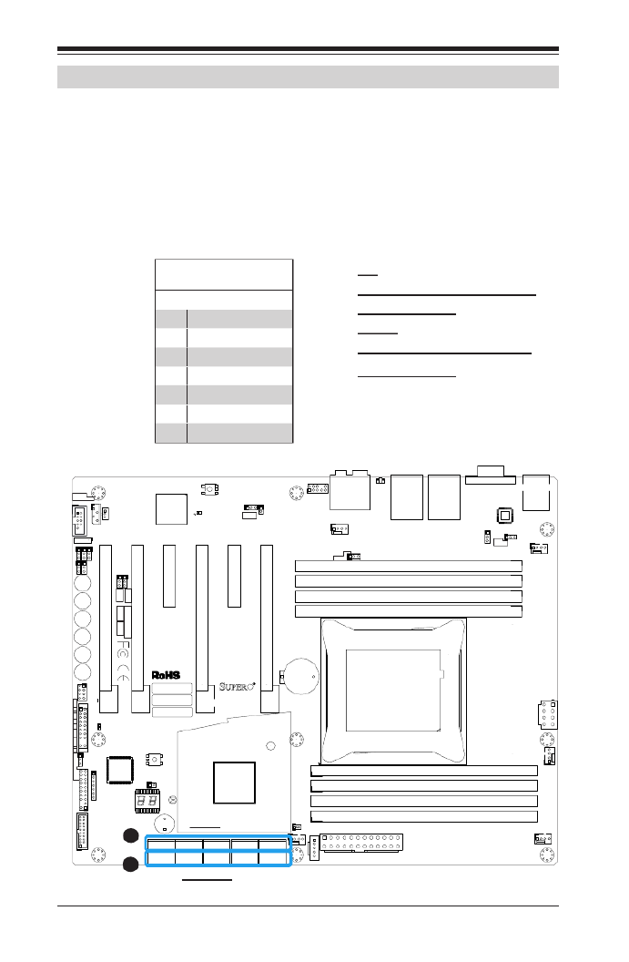
2-36
Supermicro C7X99-OCE/C7X99-OCE-F Motherboard User’s Manual
MAC CODE
IPMI CODE
BAR CODE
C7X99-OCE-F
SW_BIOSRC
S4
S7
S10
S5
S6
S9
OC_FRONT_PANEL
S8
S11
CLR_CMOS_SW
JUSB30_I2
JAUDIO1
LED4
I-SATA0I-SATA2I-SATA4S-SATA0S-SATA2
AUDIO_FP
JIPMB1
JSD1
MH11
MH2
MH9
MH10
JPW2
CA
LEDM1
JBT1
BT1
+
FAN5
FAN4
FAN1
1
FAN2
4
FAN3
JPL2
JPUSB1
J29
J30
JPME2
JPAC1
JPL1
JI2C1
JI2C2
JPB1
JPG1
JWD1
1
JL2
JL1
JD1
1
JF1
2
19
JPI2C1
JSTBY1
JTPM1
SP1
+
HD AUDIO
VGA
LAN1
LAN2
USB 16/17(3.0)
USB 12/13(3.0) USB 10/11(3.0)
USB 14/15(3.0)
CPU SLOT6 PCI-E 3.0 X16
PCH SLOT5 PCI-E 2.0 X1 (IN X4)
CPU SLOT4 PCI-E 3.0 X8 (IN X16)
PCH SLOT3 PCI-E 2.0 X1 (IN X4)
CPU SLOT2 PCI-E 3.0 X8 (IN X16)
CPU SLOT1 PCI-E 3.0 X8 (IN X16)
2-3:DISABLE
1-2:ENABLE
:WATCH DOG
SPEAKERPWR LED
:TPM/PORT80
CPU
CHASSIS INTRUSION
JI2C2
2-3:DISABLE
1-2:ENABLEJI2C1
PWR ON OH/FF NIC1NIC2RST X
CMOS CLEAR
1-2:NORMAL
2-3:BIOS RECOVERY
JBR1
PWR LEDHDD LED NMIX
2-3:ME MANUFACTURING MODE
JPME2
1-2:NORMAL
1-2 ENABLE
2-3 DISABLE
1-2 ENABLE
2-3 DISABLE
:PWR I2C
1-2 ENABLE2-3 DISABLE
2-3 DISABLE
1-2 ENABLE
1-2 ENABLE
2-3 DISABLE
JPAC1
VGA
USB14/15 WAKE UP
1-2 RST
2-3 NMI
:SATA DOM POWER
DIMMD2
DIMMD1
DIMMC2
DIMMC1
DIMMB2
DIMMB1
DIMMA2
DIMMA1
JBR1
JWD1
JPW1
JPUSB1
JPB1
JPG1
C
A
LED1
I-SATA1I-SATA3I-SATA5S-SATA1
S-SATA3
C7X99-OCE/
COM1
2-10 SATA Connections
SATA Connections (I-SATA0~5, S-SATA0~3)
Ten Serial ATA (SATA) 3.0 connectors (I-SATA0~5, S-SATA0~3) are sup-
ported on the board. All SATA 3.0 ports are supported by the Intel X99
PCH chip. RAID 0,1,5,10 are supported on I-SATA 0~5. These high
speed ports support transfer rates of up to 6Gb/s. See the table on the
right for pin denitions.
SATA 2.0/3.0 Connectors
Pin Denitions
Pin# Signal
1 Ground
2 SATA_TXP
3 SATA_TXN
4 Ground
5 SATA_RXN
6 SATA_RXP
7 Ground
Top
A. S-SATA2, S-SATA0, I-SATA4,
I-SATA2, I-SATA0
Bottom
B. S-SATA3, S-SATA1, I-SATA5,
I-SATA3, I-SATA1
A
B
(Top)
(Bottom)
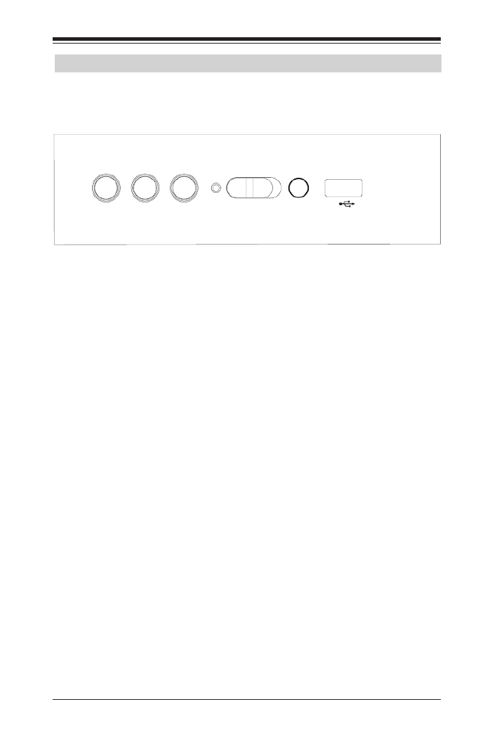
Chapter 2: Installation
2-37
2-10 The OC Front Control Panel (Optional)
The OC (Overclocking) Front Control Panel has Six (6) control buttons,
switches and one USB port.
Clean CMOS
& Reset
Boot BIOS
Switch Bios Rec eryov
BIOS1 BIOS2
OC-1 OC-2 OC-3
Boot BIOS Switch
The Boot BIOS Switch is used to select between two boot BIOS blocks
that are installed on the motherboard. See Appendix D for details.
BIOS Recovery
Push the BIOS Recovery button to enable the motherboard to enter the
BIOS Recovery process and re-install the BIOS, reverting all settings
back to factory default. It looks for a le named "SUPER.ROM" from a
memory device attached to any of the USB drives. It functions the same
way as the BIOS Restore Button which is installed on the motherboard,
see page 2-34.
Front USB Port
The Front USB Port is dened as USB 3.0 Port# XX on this motherboard.
It is conveniently located on the OC panel for quick access for USB
memory sticks and other storage devices.
Over-Clocking Buttons (OC1, OC2, OC3)
Press these buttons to activate the over-clocking feature of the motherboard. These
buttons will allow the CPU to run above its rated speed. This is an advanced feature
and should only be used by experienced users. These work the same way as the
OC buttons on the motherboard, see Page 2-32 for details.
Clear CMOS and Reset
Use the push-button hardware switch to clear the CMOS memory back to
its default values and reset the system. There is also a similar switch on
the motherboard (JBT1), but is made up of two contact pads that need
to be shorted with a metallic object (i.e., screwdriver, etc).

2-38
Supermicro C7X99-OCE/C7X99-OCE-F Motherboard User’s Manual
Installing the OC Front Control Panel
The OC Front Control Panel is designed to t into an external 5.25-inch
external drive bay of a desktop-style or tower-style computer chassis.
Make sure that the appropriate type of screws are used.
The OC Front Control panel
The OC Control panel easily slides into a standard 5.25-inch drive
bay on a desktop or tower-style computer chassis.
Make sure to secure the OC Control Panel
with the correct screws, but do not over-
tighten.
Connect all the
OC Control Panel
cables to the ap-
propriate head-
ers located on the
motherboard.
Produkt Specifikationer
| Mærke: | Supermicro |
| Kategori: | Bundkort |
| Model: | C7X99-OCE-F |
Har du brug for hjælp?
Hvis du har brug for hjælp til Supermicro C7X99-OCE-F stil et spørgsmål nedenfor, og andre brugere vil svare dig
Bundkort Supermicro Manualer

18 December 2024
6 December 2024
6 December 2024
6 December 2024
6 December 2024
6 December 2024
5 December 2024
6 Oktober 2024
4 September 2024
3 September 2024
Bundkort Manualer
- Bundkort Asus
- Bundkort Gigabyte
- Bundkort Asrock
- Bundkort MSI
- Bundkort NZXT
- Bundkort ECS
- Bundkort Sapphire
- Bundkort Intel
- Bundkort Sharkoon
- Bundkort Biostar
- Bundkort Evga
- Bundkort Foxconn
- Bundkort Advantech
- Bundkort Elitegroup
- Bundkort EPoX
- Bundkort AOpen
- Bundkort Raspberry Pi
Nyeste Bundkort Manualer
29 Marts 2025

27 Marts 2025
6 Marts 2025
15 Februar 2025

15 Februar 2025
15 Februar 2025
15 Februar 2025
15 Februar 2025
15 Februar 2025
15 Februar 2025